
Datasheet


SLUS488E − SEPTEMBER 2002 − REVISED JULY 2009
7
www.ti.com
detailed pin descriptions (continued)
OUTA and OUTB: Alternating high-current output stages. Both stages are capable of driving the gate of a power
MOSFET. Each stage is capable of 500-mA peak-source current, and 1-A peak-sink current.
The output stages switch at half the oscillator frequency, in a push-pull configuration. When the voltage on the
internal oscillator capacitor is rising, one of the two outputs is high, but during fall time, both outputs are off. This
dead time between the two outputs, along with a slower output rise time than fall time, ensures that the two
outputs cannot be on at the same time. This dead time is typically 110 ns.
The high-current output drivers consist of MOSFET output devices, which switch from VDD to GND. Each output
stage also provides a very low impedance to overshoot and undershoot. This means that in many cases,
external Schottky clamp diodes are not required.
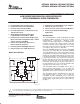
RT: The oscillator programming pin. The oscillator features an internal timing capacitor. An external resistor,
R
T
, sets a current from the RT pin to ground. Due to variations in the internal C
T
, nominal V
RT
of 1.5 V can vary
from 1.2 V to 1.6 V
Selecting RT as shown programs the oscillator frequency:
RT +
1
28.7 10
−12
ǒ
1
f
OSC
* 2.0 10
−7
Ǔ
where f
OSC
is in Hz, resistance in Ω. The recommended range of timing resistors is between 25 kΩ and 698 kΩ.
For best performance, keep the timing resistor lead from the RT pin to GND (pin 5) as short as possible.
UDG−01083
Approximate Frequency +
1
28.7 10
−12
R
T
)
ǒ
2.0 10
−7
Ǔ
4
1.5 V
0.2 V
SQ
R
I
RT
I
CT
C
T
1.5 V
OSCILLATOR
OUTPUT
R
T
Figure 2. Block Diagram for Oscillator
VDD: The power input connection for this device. Although quiescent VDD current is very low, total supply
current may be higher, depending on OUTA and OUTB current, and the programmed oscillator frequency. Total
VDD current is the sum of quiescent VDD current and the average OUT current. Knowing the operating
frequency and the MOSFET gate charge (Q
G
), average OUT current can be calculated from:
I
OUT
+ Q
G
f
OSC
where f is the oscillator frequency.
To prevent noise problems, bypass VDD to GND with a ceramic capacitor as close to the chip as possible along
with an electrolytic capacitor. A 1-µF decoupling capacitor is recommended.
(3)
(4)