
Datasheet


SLUS488E − SEPTEMBER 2002 − REVISED JULY 2009
5
www.ti.com
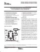
functional block diagram
UDG−01081
Q
Q
T
+
8
2
3
4
7
6
5
1CTRL
VDD
CS
ISET
GND
RT
OUTA
OUTB
0.75V
0.5V
1.5V
0.2V
SQ
R
SQ
R
0.5V
Vdd−1
VREF
SQ
R
I
SLOPE
Css
Iss
SQ
R
Soft Start and Fault Latch
PWM Comparator/Latch Output Driver
Oscillator
CS Circuitry
Slope Circuit
Bias/UVLO
I
SLOPE
=
5 x I
SET
I
CT
C
T
1.5V
C
T
80 k
Ω
60 k
Ω
0.3 V
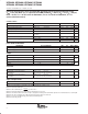
Terminal Functions
TERMINAL
NAME
PACKAGE
I/O DESCRIPTION
NAME
D OR P
I/O
DESCRIPTION
CS 3 I The current-sense input to the PWM comparator, the cycle-by-cycle peak current comparator, and the
overcurrent comparator. The overcurrent comparator is only intended for fault sensing. Exceeding the
overcurrent threshold causes a soft-start cycle. An internal MOSFET discharges the current-sense filter
capacitor to improve dynamic performance of the power converter.
CTRL 1 I Error voltage input to PWM comparator.
GND 5 − Reference ground and power ground for all functions. Due to high currents, and high-frequency operation
of the IC, a low-impedance circuit board ground plane is highly recommended.
ISET 2 I Current selection for slope compensation.
OUTA 7 O
Alternating high-current output stages.
OUTB 6 O
Alternating high-current output stages.
RT 4 I Programs the oscillator.
VDD 8 I Power input connection.