
Datasheet


10 1 11 13
9
2
5
4
3
8
6
12147
TST VDD NC PFCDRV
VBULK
CS
LINESNS
CS
BIAS
CTRL
VSSNC
BIASSNS
FAULT
REFIN
R86
300 kW
C80
100 nF
TP4
C78
470 nF
R75
143 kW
5%
U13
TLVH431ACDBZR
R76
30 kW
5%
R76
14.3 kW
4
2
5
GND
VIN OUT
U10
TPS71533DCKR
U1
UCC29910APW
R77
1 M
R80
390 W
R5
10 kW
R85
56 kW
R84
680 kW
C45
100 mF
16 V
HV
V
PRI
VCCA
V
DD_3V
Q12
BSS126
UDG-11108
UCC29910A
SLUSAK8A –MAY 2011– REVISED JUNE 2011
www.ti.com
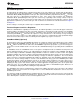
Start-Up With External FET
Conventional start-up schemes utilising either resistive or enhancement mode MOSFET feeds incur line
dependant static power losses. To avoid these power losses and to obtain an optimum turn-on time an external
depletion mode FET may be used Figure 5 and Figure 6. The V
HV
node is connected to the rectified incoming
line. Q12 is a depletion mode FET which will start charging C45 as soon as line power is connected. Initially U1
is inactive and BIASCTRL is low. The VDD_3V rail will begin to increase as U10 starts to conduct. The POR
(Power On Reset) sequence of U1 will begin once this rail gets to about 1.7 V and will execute while the
VDD_3V rail is being established. The BIASCTRL pin will go high when BIASSNS reaches the V
B(max)
level. If
VLINESNS is then > V
BH
, U1 begins to pulse the PFCDRV pin, which starts the process of charging the bulk
capacitors at the output of the buck PFC power stage. The PFCDRV current is drawn from C45, which starts to
discharge. If the voltage at the BIASSNS pin falls below V
B(min)
then PFC switching is disabled and Q12 is turned
on to re-charge C45. With the given component values the V
B(max)
level corresponds to 12 V and a V
B(min)
level of
6 V at the V
CCA
rail. The user sets the V
B(max)
and V
B(min)
levels depending on the characteristics of any
alternative components used by adjusting R84.
Figure 5. Simplified Schematic
12 Submit Documentation Feedback Copyright © 2011, Texas Instruments Incorporated
Product Folder Link(s): UCC29910A