
Datasheet


UCC2897A
SLUS829D -- AUGUST 2008 -- REVISED JULY 2009
2
www.ti.com
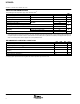
ABSOLUTE MAXIMUM RATINGS
over operating free-air temperature range unless otherwise noted
(1)
UNIT
Line input voltage, V
IN
120 V
Supply voltage, V
DD
(I
DD
<10mA) 16.5 V
Analog inputs FB, CS, SYNC, LINEOV, LINEUV --0.3to(V
REF
+0.3) V
Output source current (peak), I
O_SOURCE
O
U
T
A
U
X
2.5
A
Output sink current (peak), I
O_SINK
OUT,
A
U
X
-- 2 . 5
A
Operating junction temperature range, T
J
--55 to 150
°
C
Storage temperature, T
stg
--65 to 150
°C
E
S
D
r
a
t
i
n
g
Human body model, (HBM) 2000
V
ESD rating
Charged device m odel (CDM) 500
V
Lead temperature, T
sol,
1,6 mm (1/16 inch) from case for 10 seconds 300 °C
(2)
Stresses beyond those listed under “absolute maximum ratings” may cause permanent damage to the device. These are stress ratings only,
and functional operation of the device at thes e or any other conditions beyond those indicated under “recommended operating conditions” is
not implied. Exposure to absolute-maximum-rated conditions for extended periods may affect device reliability. All voltages are with respect to
GND. Currents are positive into and negative out of, the specified terminal.
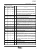
RECOMMENDED OPERATING CONDITIONS
MIN NOM MAX UNIT
Line input voltage, V
IN
18 110 V
Supply voltage, V
DD
8.5 12.0 16.0 V
Supply bypass capacitance, VDD
(2)
1 μF
Timing resistance, R
ON
=R
OFF
(for 250-kHz
operation)
75 kΩ
Operating junction temperature, T
J
-- 4 0 125 °C
Reference bypass capacitance, C
REF
0.1 μF
(2)
Supply bypass capacitance should be greater than VREF capacitance by at least 10 times.