
Datasheet


UCC1895, UCC2895, UCC3895
www.ti.com
SLUS157P –DECEMBER 1999–REVISED JUNE 2013
TERMINAL FUNCTIONS (continued)
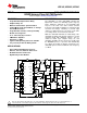
TERMINAL
I/O DESCRIPTION
NAME NO.
OUTA 18 O
OUTB 17 O
The four outputs are 100-mA complementary MOS drivers, and are optimized to drive FET driver circuits
such as UCC27424 or gate drive transformers.
OUTC 14 O
OUTD 13 O
PGND 16 - Output stage ground.
RAMP 3 I Inverting input of the PWM comparator.
5 V, ±1.2%, 5 mA voltage reference. For best performance, bypass with a 0.1-μF low ESR, low ESL
REF 4 O
capacitor to ground. Do not use more than 4.7 μF of total capacitance on this pin.
RT 8 I Oscillator timing resistor for programming the switching frequency.
SS/DISB 19 I Soft-start and disable pin which combines the two independent functions.
SYNC 6 I/O The oscillator synchronization pin is bidirectional.
The power supply input pin, VDD, must be bypassed with a minimum of a 1-μF low ESR, low ESL capacitor
VDD 15 I
to ground. The addition of a 10-μF low ESR, low ESL between VDD and PGND is recommended.
Copyright © 1999–2013, Texas Instruments Incorporated Submit Documentation Feedback 7
Product Folder Links: UCC1895 UCC2895 UCC3895