
Datasheet


3
18
17
16
EAN
12 20 19
15
14
4
5
6
7
8
9 1110 12 13
EAOUT
RAMP
EAP
SS/DISB
OUTA
OUTB
OUTC
OUTD
PGND
REF
GND
SYNC
CT
RT
VDD
CS
ADS
DELAB
DELCD
OUTA
SS/DISB
EAP
OUTB
PGND
OUTC
VDD
OUTD
EAOUT
EAN
RT
SYNC
CT
RAMP
REF
GND
DELCD
DELAB CS
20
19
18
17
16
15
14
13
12
11
1
2
3
4
5
6
7
8
9
10 ADS
1
2
3
4
5
6
7
8
9
10
20
19
18
17
16
15
14
13
12
11
EAN
EAOUT
RAMP
REF
GND
SYNC
CT
RT
DELAB
DELCD
EAP
SS/DISB
OUTA
OUTB
PGND
VDD
OUTC
OUTD
CS
ADS
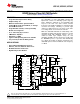
PW and DW PACKAGE
(TOP VIEW)
UCC1895, UCC2895, UCC3895
SLUS157P –DECEMBER 1999–REVISED JUNE 2013
www.ti.com
DEVICE INFORMATION
PW AND DW PACKAGE DRAWINGS N AND J PACKAGE DRAWINGS
(TOP VIEW) (TOP VIEW)
FN AND FK PACKAGE DRAWINGS
(TOP VIEW)
TERMINAL FUNCTIONS
TERMINAL
I/O DESCRIPTION
NAME NO.
The adaptive-delay-set pin sets the ratio between the maximum and minimum programmed output delay
ADS 11 I
dead time.
CS 12 I Current sense input for cycle-by-cycle current limiting and for over-current comparator.
Oscillator timing capacitor for programming the switching frequency. The UCC3895 oscillator charges CT via
CT 7 I
a programmed current.
The delay-programming between complementary-outputs pin, DELAB, programs the dead time between
DELAB 9 I
switching of output A and output B.
The delay-programming between complementary-outputs pin, DELCD, programs the dead time between
DELCD 10 I
switching of output C and output D.
EAOUT 2 I/O Error amplifier output.
EAP 20 I Non-inverting input to the error amplifier. Keep below 3.6 V for proper operation.
EAN 1 I Inverting input to the error amplifier. Keep below 3.6 V for proper operation.
GND 5 - Chip ground for all circuits except the output stages.
6 Submit Documentation Feedback Copyright © 1999–2013, Texas Instruments Incorporated
Product Folder Links: UCC1895 UCC2895 UCC3895