
Datasheet


C
BULK
C
VGG
R
ZCD2
R
ZCD1
R
CL
R
START
R
MOT
R
FB
C
VDD
D
BIAS
+
-
V
OUT
VDD
VGG
ZCD
FB
CL DRV
GND
MOT
UCC28610
V
IN
AC
D
1
C
BP
N
P
N
B
N
S
Q
1
UCC28610
SLUS888F –JANUARY 2009–REVISED SEPTEMBER 2012
www.ti.com
This integrated circuit can be damaged by ESD. Texas Instruments recommends that all integrated circuits be handled with
appropriate precautions. Failure to observe proper handling and installation procedures can cause damage.
ESD damage can range from subtle performance degradation to complete device failure. Precision integrated circuits may be more
susceptible to damage because very small parametric changes could cause the device not to meet its published specifications.
ORDERING INFORMATION
OPERATING
PACKAGE ORDERABLE PART
TEMPERATURE PINS PACKAGE TRANSPORT MEDIA UNITS
LEAD NUMBER
RANGE, T
A
8 Plastic Small Outline SOIC D Tape and Reel 2500 UCC28610DR
–40°C to 125°C
8 Plastic Dual In-Line PDIP P Tube 50 UCC28610P
RECOMMENDED OPERATING CONDITIONS
Unless otherwise noted, all voltages are with respect to GND, -40°C < T
J
= T
A
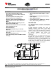
< 125°C. Components reference, Figure 1.
MIN MAX UNIT
VDD Input voltage 9 20 V
VGG Input voltage from low-impedance source 9 13
I
VGG
Input current from a high-impedance source 10 2000 μA
R
MOT
Resistor to GND Shutdown/Retry mode 25 100
Latch-off mode 150 750
kΩ
R
CL
Resistor to GND 24.3 100
R
ZCD1
Resistor to auxiliary winding 50 200
C
VGG
VGG capacitor 33 200 nF
C
BP
VDD bypass capacitor, ceramic 0.1 1 μF
Figure 1. Recommended Operating Conditions Application
2 Submit Documentation Feedback Copyright © 2009–2012, Texas Instruments Incorporated
Product Folder Links: UCC28610