
Datasheet


5
4
1
32
R1
R2
VOUT
VOUTS
GND
6 7
VIN VIN VIN VIN
CIN
VIN
8
CT
SD/CT
COUT
VOUT
+
+
(+)(+)
(−)
C1
UCC384−ADJ
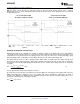
TTL SHUTDOWN CIRCUIT
1
µ
F
0.015
µ
F
4.7
µ
F
470 k
+5 V
LOGIC
INPUT
+5 V
GND
(−)
controlling the SD/CT pin
UCC284-EP
SLVS862A – NOVEMBER 2008 – REVISED NOVEMBER 2008 .......................................................................................................................................
www.ti.com
Figure 8. TTL Controlled Shutdown Circuit
Forcing the SD/CT pin to any fixed voltage affects the operation of the circuit. As mentioned before, pulling the
SD/CT pin more positive than – 0.7 V puts the circuit in a shutdown mode, limiting the quiescent current to less
than 45 µ A. Pulling this pin more positive than 6 V with respect to GND damages the device.
Forcing the SD/CT pin to any fixed voltage between – 0.7 V and – 1.6 V with respect to GND enables the output.
However, in an overcurrent condition, the output does not pulse at a 2.5% duty cycle, but the output current is
still limited to the peak current limit. This circuit may be used where a fixed current limit is needed, where a 2.5%
duty cycle is undesirable. The UCC284 supplies a maximum current in this configuration as long as the
temperature of the device does not exceed the overtemperature shutdown. This is determined by the peak
current being supplied, the input and output voltages, and the type of heat sink being used. Thermal design is
discussed later on in this data sheet.
Forcing the SD/CT pin to a voltage level between approximately – 1.6 V and – 2.6 V with respect to GND is not
recommended as the output may or may not be enabled.
Forcing the SD/CT pin to a voltage level between approximately – 2.6 V and – 5 V with respect to GND turns the
output off completely. The output remains off as long as the voltage is applied. Pulling this pin more negative
than – 5 V with respect to GND damages the device (see Table 1 ).
Table 1. SD/CT Voltage Levels
SD/CT STATE
6 V to – 0.7 V Output disabled and device in low quiescent shutdown mode.
– 0.7 V to – 1.6 V Output enabled
– 1.6 V to – 2.6 V Output enabled or disabled depending on the previous state.
– 2.6 V to – 5 V Output disabled
12 Submit Documentation Feedback Copyright © 2008, Texas Instruments Incorporated
Product Folder Link(s): UCC284-EP