
Datasheet


SLUS168D – APRIL 1999 – REVISED AUGUST 2002
3
www.ti.com
electrical characteristics, T
A
= 0°C to 70°C for the UCC3808–x, –40°C to 85°C for the UCC2808–x and –55°C
to 125°C for the UCC1808–x, VDD = 10 V (See Note 6), 1 µF capacitor from VDD to GND, R = 22 kΩ, C = 330 pF,
T
A
= T
J
, (unless otherwise specified)
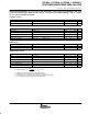
oscillator section
PARAMETER TEST CONDITIONS MIN TYP MAX UNITS
Oscillator frequency 175 194 213 kHz
Oscillator amplitude/VDD See Note 1 0.44 0.5 0.56 V/V
error amplifier section
PARAMETER TEST CONDITIONS MIN TYP MAX UNITS
Input voltage COMP = 2 V 1.95 2 2.05 V
Input bias current –1 1 µA
Open loop voltage gain 60 80 dB
COMP sink current FB = 2.2 V, COMP = 1 V 0.3 2.5 mA
COMP source current FB = 1.3 V, COMP = 3.5 V –0.2 –0.5 mA
PWM section
PARAMETER TEST CONDITIONS MIN TYP MAX UNITS
Maximum duty cycle Measured at OUTA or OUTB 48% 49% 50%
Minimum duty cycle COMP = 0 V 0%
current sense section
PARAMETER TEST CONDITIONS MIN TYP MAX UNITS
Gain See Note 2 1.9 2.2 2.5 V/V
Maximum input signal COMP = 5 V, See Note 3 0.45 0.5 0.55 V
CS to output delay COMP = 3.5 V, CS from 0 to 600 mV 100 200 ns
CS source current –200 nA
Over current threshold 0.7 0.75 0.8 V
COMP to CS offset CS = 0 V 0.35 0.8 1.2 V
NOTES: 1. Measured at RC. Signal amplitude tracks VDD.
2. Gain is defined by: A +
DV
COMP
DV
CS
,0v V
CS
v 0.4 V,
3. Parameter measured at trip point of latch with FB at 0V.
4. Start threshold and zener shunt threshold track one another.
5. For UCCx808–1, set VDD above the start threshold before setting at 10 V.
6. Does not include current in the external oscillator network.