
Datasheet


VREF
R
OH
R
OL
Gate
Voltage
Boost
Narrow Pulse at
each Turn On
Anti Shoot -
Through
Circuitry
Input Signal
R
NMOS
, Pull Up
OUTL
OUTH
UCC27611
www.ti.com
SLUSBA5B –DECEMBER 2012
Enable Function
As mentioned earlier, an enable and disable function can be easily implemented in UCC27611 using the unused
input pin. When IN+ is pulled down to GND or IN- is pulled down to VDD, the output is disabled. Thus IN+ pin
can be used like an enable pin that is based on active high logic, while IN- can be used like an enable pin that is
based on active low logic.
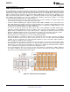
Output Stage
The output stage of the UCC27611 device is illustrated in Figure 14. OUTH and OUTL are externally connected
and pinned out as OUTH and OUTL pins. The UCC27611 device features a unique architecture on the output
stage which delivers the highest peak source current when it is most needed during the Miller plateau region of
the power switch turn-on transition (when the power switch drain and collector voltage experiences dV and dt).
The device output stage features a hybrid pull-up structure using a parallel arrangement of N-channel and P-
channel MOSFET devices. By turning on the N-channel MOSFET during a narrow instant when the output
changes state from low to high, the gate-driver device is able to deliver a brief boost in the peak-sourcing current
enabling fast turn on.
Figure 14. UCC27611 Gate Driver Output Structure
The R
OH
parameter (see ELECTRICAL CHARACTERISTICS) is a DC measurement and it is representative of
the on-resistance of the P-channel device only, since the N-channel device is turned on only during output
change of state from low to high. Thus the effective resistance of the hybrid pull-up stage is much lower than
what is represented by ROH parameter. The pull-down structure is composed of a N-channel MOSFET only. The
R
OL
parameter (see ELECTRICAL CHARACTERISTICS), which is also a DC measurement, is representative of
true impedance of the pull-down stage in the device.
The UCC27611 is capable of delivering 4-A source, 6-A sink (asymmetrical drive) at VDD = 12 V. Strong sink
capability in asymmetrical drive results in a very low pull-down impedance in the driver output stage which boosts
immunity against parasitic, Miller turn on (C x dV/dt turn on) effect, especially where low gate-charge MOSFETs
or emerging wide band-gap GaN power switches are used.
Copyright © 2012, Texas Instruments Incorporated Submit Documentation Feedback 13
Product Folder Links: UCC27611