
Datasheet


9
UCC2750
UCC3750
problem is only manifested for high values of VB (e.g.
48V) and can be alleviated by using a fraction of the re
-
quired DC offset as the VB input and regaining the offset
with resistive ratios.
The error amplifier compares the reference signal with
the output voltage by way of weighted sum at its inverting
input. The error signal is further processed to separate its
polarity and magnitude. An absolute value circuit (preci
-
sion full-wave rectifier) is used to get the magnitude infor
-
mation. The polarity is used along with the reference
signal polarity to determine the mode information. The
absolute value circuit provides phase inversion when ap
-
propriate for modes 2 and 3 to maintain the correct loop
gain polarity. While the output of the error amplifier
swings around 3V, the full-wave rectifier output (MAG)
converts it into a signal above 3V. This signal is com
-
pared to the oscillator ramp to generate the PWM output.
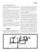
Oscillator and PWM Comparator
The UCC3750 has an internal oscillator capable of high
frequency (>250kHz) operation. A resistor on the RT pin
programs the current that charges and discharges CT,
resulting in a triangular ramp waveform. Fig 7. shows the
oscillator hook-up circuit. The ramp peak and valley are
4.75V and 3V respectively. The nominal frequency is
given by:
f=
1
1.17• RT• CT
OS C
The ramp waveform and the rectified output of the error
amplifier are compared by the PWM comparator to gen
-
erate the PWM signal. The PWM action is disabled on
the positive slope of the ramp signal. Leading edge mod
-
ulation turns on the PWM signal when the ramp signal
falls below MAG on the falling slope and turns it off at the
end of the clock cycle. This technique enables synchro
-
nized turn-on of the rectifier switches immediately after
the PWM pulse is turned off. The triangular nature of the
ramp ensures that the maximum duty cycle of the PWM
output is 50%, providing inherent current limiting.
Control Logic and Outputs
The PWM signal is processed through control logic which
takes into account the operating mode and output polar
-
ity to determine which output to modulate. The logic table
for the outputs is given in Table 2. For example, assume
that the reference signal is in the first quadrant (positive
and increasing). The output will lag the reference by a
certain delay and hence the error amp output will be pos
-
itive, resulting in SIGN = 0. The logic table indicates that
GD1 is modulated during this phase allowing power
transfer to increase the output voltage to keep up with
the reference. Increasing error (MAG) will result in larger
duty cycle and enable the output to increase and catch
up with the reference. If the output becomes higher than
the reference (as is likely in the second quadrant when
the reference is dropping), the SIGN becomes 1 and
GD3 is modulated to decrease the output level by trans-
ferring power to the input. At the boundary of the first and
second quadrant, there may be some switching back and
forth between modes as the reference slope crosses
through zero. Some of this switching can be eliminated
by judicious selection of error amplifier filtering and com
-
pensation components. In the first quadrant, when PWM
is applied to Q1, Q2 is turned on in the rectifier mode by
the clock signal to allow the flyback transformer flux to
APPLICATION INFORMATION (cont.)
24
23
CT
+
–
I
R
S
Q
R
+
–
I
R
C
T
RT
3V
I
R
R
T
4.75V
3.0V
Figure 7. Oscillator setup.
UDG-99077