
Datasheet


4
UCC2750
UCC3750
GD2: Output driver that controls the p-channel secondary
side switch in the flyback converter. The output signal on
this pin is PWM during mode 4 (Fig. 2) when the
reference signal is negative and power is being returned
to the input. This pin functions as a synchronous rectifier
output during mode 1 with positive reference signal and
positive power transfer. This output is logically inverted to
provide the correct polarity drive signal for a p-channel
switch.
GD3: Output driver that controls the n-channel secondary
side switch in the flyback converter. The output signal on
this pin is PWM during mode 2 (Fig. 2) when the
reference signal is positive and power is being returned
to the input. This pin functions as a synchronous rectifier
output during mode 3 with a negative reference signal
and positive power transfer.
GND: Reference point for the internal reference and all
thresholds. Also provides the signal return path for all
other pins.
NEG1: Inverting input of the buffer amplifier that acts as
a summing junction for the DC (battery) offset voltage
and sinewave reference.
NEG2: Inverting input of the error amplifier where the
ringer output voltage and the reference signal with the
desired offset are applied with a weighted sum.
Feedback compensation is connected between NEG2
and OUT2.
NEGDC: Inverting input of the amplifier used for DC
current limiting.
OUT1: Output of the buffer amplifier that provides scaling
and filtering for the reference signal before feeding it into
the error amplifier. This output is also used internally to
select the PWM mode for the flyback converter.
OUT2: Output of the error amplifier. Used to connect
compensation components. This output’s absolute value
determines the duty cycle of the PWM pulse. The polarity
of this signal also determines the PWM mode.
OUTDC: Output of the DC current limit amplifier. The DC
current limit is activated when this pin is above 4.5V or
below 1.5V.
REF: Internal 7.5V reference. For best results, bypass to
GND with a ceramic capacitor(>0.1µF).
RGOOD: Logic output that indicates that the error
amplifier output is within range (0< D< 0.5). This pin can
source upto 0.5mA of current.
RT: Resistor from RT to GND helps set the oscillator
frequency. RT programs the charge and discharge
currents of CT.
SINFLT: This signal is the buffered version of SINREF.
This signal is summed with the DC offset level with
appropriate scaling.
SINREF: This pin is the output of the sine-wave
reference generator. It has a high output impedance
(≈25kΩ). A 0.01µF capacitor to GND is recommended to
provide smoothing of the sinewave. When FS0 and FS1
are both set high, the sine reference generator is
disabled allowing this pin to accept an external sinewave
input.
SWRLY: Logic output that leads the battery offset
crossings (by typically 5ms) to allow “zero voltage” relay
switching. This pin can typically source 250µA.
XTAL1: Crystal connection for external crystal. This pin
can be also used to clock the internal sine wave
generator when XTAL2 is connected to VDD/2.
XTAL2:Crystal connection for external crystal.
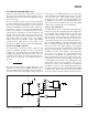
VCP: External connection for charge pump storage
capacitor. A capacitance ≥2.2mF is recommended for
low charge pump output ripple. The voltage at this pin is
used by the output drivers for gate drive voltages.
Alternatively, a regulated gate drive voltage (>10V) can
be connected at this pin while leaving the charge pump
circuit at nodes VS1, VS2 disconnected.
VDD: External supply input used to bias internal logic
functions. Typically a regulated 5V supply is connected
between this pin and GND. It also is the input voltage for
the voltage tripler circuit to generate the gate drive
voltage.
VS1, VS2: Voltage switches for the voltage tripler
(charge pump circuit). They provide different voltage
levels to external capacitors in order to pump up the
voltage from VDD to VCP.
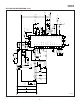
PIN DESCRIPTIONS (cont.)