
Datasheet


3
UCC2750
UCC3750
ELECTRICAL CHARACTERISTICS:
Unless otherwise stated, these specifications apply for T
A
= 0°C to 70°C for the
UCC3750, –40°C to +85°C for the UCC2750, RT = 14k, CT = 470pF, C
REF
= 0.1µF, FS0 = 0, FS1 = 0, VDD = 5V. T
A
=T
J
.
PARAMETER TEST CONDITIONS MIN TYP MAX UNITS
Oscillator
Accuracy 108 128 148 kHz
Peak Voltage 4.6 4.75 4.9 V
Valley Voltage 2.9 3.05 3.2 V
Charge Pump
Switch Pull Up Resistance (VS1, VS2) 10 30 Ω
Switch Pull Down Resistance (VS1, VS2) 10 30 Ω
Output Voltage (VCP) VDD = 5V, I
VCP
= 10mA 11 12 14 V
Output Drivers
Pull Up Resistance 915Ω
Pull Down Resistance 915Ω
Rise Time CL = 2.7nF 50 100 ns
Fall Time CL = 2.7nF 50 100 ns
Current Limit
DC Limit Threshold Voltage Positive R5/R6 = 3 0.4 0.5 0.6 V
DC Limit Threshold Voltage Negative R5/R6 = 3 –0.6 –0.5 –0.4 V
Duty Cycle
Maximum PWM Duty Cycle 48 50 %
Rectifier Duty Cycle 50 %
Note 1: Guaranteed by measuring the steps of the PWL Sine Wave.
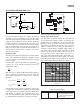
STATE % VCC VALUE FOR REF = 7.5 STATE % VCC VALUE FOR REF = 7.5
0 0.3333 2.5 5 0.4255 3.191
1 0.3384 2.538 6 0.4471 3.353
2 0.3528 2.646 7 0.4616 3.462
3 0.3745 2.808 8 0.4666 3.5
4 0.4 3
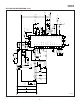
AMPIN: Inverting input of the uncommitted amplifier.
AMPOUT: Output of the uncommitted amplifier.
CT: This pin programs the internal PWM oscillator
frequency. Capacitor from CT to GND sets the charge
and discharge time of the oscillator.
ENBL: Logic input which enables the outputs and the
charge pump when high. ENBL should be pulled low to
turn the outputs off.
FS0, FS1: Frequency select pins for the internal
sine-wave generator. Table 1 provides the SINREF
frequencies as a function of FS0 and FS1 when a 32kHz
crystal is used at the crystal inputs (XTAL1, XTAL2).
Other proportional frequencies can be obtained with a
different crystal. Inputs FS0 and FS1 are TTL compatible.
Table I. Frequency selection table
(for 32kHz crystal).
FS0 FS1 SINREF (Hz)
00 20
10 25
01 50
1 1 High Impedance
GD1: Output driver that controls the primary side switch
in a flyback converter through a gate drive transformer.
The output signal on this pin is PWM during positive
power transfer modes and zero during negative power
transfer modes.
PIN DESCRIPTIONS