
Datasheet


2
UCC2750
UCC3750
ABSOLUTE MAXIMUM RATINGS
Input Supply Voltage
VDD........................................7.5V
Maximum Forced Voltage
VCP................................–0.3V to 13.2V
VS1, VS2...............................–0.3V to 5V
OUT1, OUT2, AMPOUT, OUTDC
Maximum Forced Voltage ................–0.3V to 7.5V
Maximum Forced Current ..............Internally Limited
NEG1, NEG2, AMPIN, NEGDC
Maximum Forced Voltage ................–0.3V to 7.5V
SINREF, SINFLT
Maximum Forced Voltage ................–0.3V to 7.5V
Logic Inputs
Maximum Forced Voltage ................–0.3V to 7.5V
Reference Output Current (REF) ..........Internally Limited
Output Current (GD1, GD2, GD3)
Pulsed.......................................1.5A
Storage Temperature ...................–65°C to +150°C
Junction Temperature...................–55°C to +150°C
Lead Temperature (Soldering, 10 Sec.).............+300°C
Unless otherwise indicated, voltages are reference to ground
and currents are positive into, negative out of the specified ter
-
minal. Pulsed is defined as a less than 10% duty cycle with a
maximum duration of 500ns. Consult Packaging Section of
Databook for thermal limitations and considerations of pack-
ages.
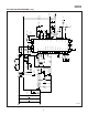
OUTDC
REF
GD3
ENBL
FS 1
RT
CT
XTAL1
GD2
GND
GD1
SINFLT
VDD
SINREF
VCP
VS 1
VS 2
RGOOD
SWRLY
NEGDC NEG1
XTAL2
FS 0
NEG2
AMP O UT
AMP IN O UT2
OUT1
14
13
12
11
10
9
8
7
6
5
4
3
2
1
15
16
17
18
19
20
21
22
23
24
25
26
27
28
CONNECTION DIAGRAM
DIL-28, SOIC- 28 (Top View)
N Package, DW Package
ELECTRICAL CHARACTERISTICS:Unless otherwise stated, these specifications apply for T
A
= 0°C to 70°C for the
UCC3750, –40°C to +85°C for the UCC2750, RT = 14k, CT = 470pF, C
REF
= 0.1µF, FS0 = 0, FS1 = 0, VDD = 5V. T
A
=T
J
.
PARAMETER TEST CONDITIONS MIN TYP MAX UNITS
VDD Supply
Supply Current - Active With 12V Supplied to V
CP
and Charge Pump
Disabled
0.5 1 mA
Internal Reference w/External Bypass
Output Voltage (REF) 7.3 7.55 7.8 V
Load Regulation I
REF
= 0mA – 2mA 30 60 mV
Line Regulation VCP = 10V to 13V, I
REF
= 1mA 3 15 mV
Amplifier
Input Voltage Error, DC Offset and Amp Amplifiers 2.9 3 3.1 V
DC Limit Amplifier 0.7125 0.75 0.7875 V
Input Bias Current 15 100 nA
AVOL V
OUT
=2Vto4V 70 dB
VOH Source 100µA 5.35 6 7.0 V
VOL Sink 100µA 0.2 0.65 V
Short Circuit Current V
IN
= 0V and 5V with V
OUT
= 0V and 5V 0.5 2 3 mA
Sine Reference
Accuracy T
J
= 25°C, Program Frequency–Reference
Frequency
–1 0 1 Hz
Total Harmonic Distortion (Note 1) 2 %
Amplitude Peak 0.475 0.5 0.525 V
Offset 2.85 3.0 3.15 V