
Datasheet


UDG-01067
UCC27423
GND
1
2
3
4
INB
INA
7
6
5
8
OUTA
VDD
OUTB
INPUT
1
µ
F
CER
2.2µF
VDD
ENBB
ENBA
C
LOAD
UDG-01066
UCC27423
GND
1
2
3
4
INB
INA
7
6
5
8
OUTA
VDD
OUTB
INPUT
1 µF
CER
100
µ
F
AL EL
D
SCHOTTKY
VDD
C2
1
µ
F
V
SNS
R
SNS
0.1
Ω
C3
100
µ
F
10Ω
+
D
ADJ
5.5 V
ENBB
ENBA
UCC27423, UCC27424, UCC27425
SLUS545D –NOVEMBER 2002–REVISED MAY 2013
www.ti.com
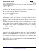
Figure 4.
Operational Waveforms and Circuit Layout
Figure 5 shows the circuit performance achievable with a single driver (1/2 of the 8-pin IC) driving a 10-nF load.
The input pulsewidth (not shown) is set to 300ns to show both transitions in the output waveform. Note the linear
rise and fall edges of the switching waveforms. This is due to the constant output current characteristic of the
driver as opposed to the resistive output impedance of traditional MOSFET-based gate drivers.
Figure 5.
8 Submit Documentation Feedback Copyright © 2002–2013, Texas Instruments Incorporated
Product Folder Links: UCC27423 UCC27424 UCC27425