
Datasheet


2
UC2855A/B
UC3855A/B
ABSOLUTE MAXIMUM RATINGS
Supply Voltage VCC..........................Internally Limited
VCC Supply Clamp Current .......................20mA
PFC Gate Driver Current (continuous) ..............±0.5A
PFC Gate Driver Current (peak) ...................±1.5A
ZVT Drive Current (continuous
) ...................±0.25A
ZVT Drive Current (peak
)........................±0.75A
Input Current (IAC, RT, RVA) .......................5mA
Analog Inputs (except Peak Limit)..............−0.3 to 10V
Peak Limit Input ...........................−0.3 to 6.5V
Softstart Sinking Current .........................1.5mA
Storage Temperature ...................−65°C to +150°C
Junction Temperature...................−55°C to +150°C
Lead Temperature (Soldering, 10 sec.) .............+300°C
Currents are positive into, negative out of the specified termi
-
nal. Consult Packaging Section of Databook for thermal limita
-
tions and considerations of packages. All voltages are
referenced to GND.
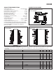
CONNECTION DIAGRAMS
PLCC-20 & LCC-20 (Top View)
Q or L Package
DIL–20 (Top View)
J or N Package
SOIC-20 (Top View)
DW Package
ELECTRICAL CHARACTERISTICS:Unless otherwise specified: VCC = 18V, RVS = 23k, CT = 470pF, CI = 150pF, VRMS
= 1.5V, IAC = 100µA, I
SENSE
= 0V, CAO = 4V, VAOUT= 3.5V, VSENSE = 3V. –40°C to 85°C (UC2855A/B), 0°Cto70°C
(UC3855A/B).
PARAMETER TEST CONDITIONS MIN TYP MAX UNITS
Overall
Supply Current, OFF CAO, VAOUT = 0V, VCC = UVLO −0.3V 150 500 µA
Supply Current, OPERATING 17 25 mA
VCC Turn-On Threshold UC3855A 15.5 17.5 V
VCCTurn-Off Threshold UC3855A,B 9 10 V
VCC Turn-On Threshold UC3855B 10.5 10.8 V
VCC Clamp I(VCC) = I
CC(on)
+ 5mA 18 20 22 V
Voltage Amplifier
Input Voltage 2.9 3.1 V
VSENSE Bias Current −500 25 500 nA
Open Loop Gain V
OUT
=2to5V 65 80 dB
V
OUT
High I
LOAD
= –300µA 5.75 6 6.25 V
V
OUT
Low I
LOAD
= 300µA 0.3 0.5 V
Output Short Circuit Current VOUT = 0V 0.6 3 mA