
Datasheet


TXS0102
www.ti.com
SCES640D –JANUARY 2007– REVISED MARCH 2011
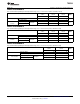
ABSOLUTE MAXIMUM RATINGS
(1)
over recommended operating free-air temperature range (unless otherwise noted)
MIN MAX UNIT
V
CCA
Supply voltage range –0.5 4.6 V
V
CCB
Supply voltage range –0.5 6.5 V
A port –0.5 4.6
V
I
Input voltage range
(2)
V
B port –0.5 6.5
A port –0.5 4.6
Voltage range applied to any output
V
O
V
in the high-impedance or power-off state
(2)
B port –0.5 6.5
A port –0.5 V
CCA
+ 0.5
V
O
Voltage range applied to any output in the high or low state
(2) (3)
V
B port –0.5 V
CCB
+ 0.5
I
IK
Input clamp current V
I
< 0 –50 mA
I
OK
Output clamp current V
O
< 0 –50 mA
I
O
Continuous output current ±50 mA
Continuous current through V
CCA
, V
CCB
, or GND ±100 mA
DCT package 220
DCU package 227
θ
JA
Package thermal impedance
(4)
DQE package 261 °C/W
DQM package TBD
YZP package 102
T
stg
Storage temperature range –65 150 °C
(1) Stresses beyond those listed under "absolute maximum ratings" may cause permanent damage to the device. These are stress ratings
only, and functional operation of the device at these or any other conditions beyond those indicated under "recommended operating
conditions" is not implied. Exposure to absolute-maximum-rated conditions for extended periods may affect device reliability.
(2) The input and output negative-voltage ratings may be exceeded if the input and output current ratings are observed.
(3) The value of V
CCA
and V
CCB
are provided in the recommended operating conditions table.
(4) The package thermal impedance is calculated in accordance with JESD 51-7.
RECOMMENDED OPERATING CONDITIONS
(1) (2)
V
CCA
V
CCB
MIN MAX UNIT
V
CCA
Supply voltage
(3)
1.65 3.6 V
V
CCB
Supply voltage 2.3 5.5 V
1.65 V to 1.95 V V
CCI
– 0.2 V
CCI
A-port I/Os 2.3 V to 5.5 V
2.3 V to 3.6 V V
CCI
– 0.4 V
CCI
High-level
V
IH
V
input voltage
B-port I/Os V
CCI
– 0.4 V
CCI
1.65 V to 3.6 V 2.3 V to 5.5 V
OE input V
CCA
× 0.65 5.5
A-port I/Os 0 0.15
Low-level
V
IL
(4)
B-port I/Os 1.65 V to 3.6 V 2.3 V to 5.5 V 0 0.15 V
input voltage
OE input 0 V
CCA
× 0.35
A-port I/Os, push-pull driving 10
Input transition
Δt/Δv B-port I/Os, push-pull driving 1.65 V to 3.6 V 2.3 V to 5.5 V 10 ns/V
rise or fall rate
Control input 10
T
A
Operating free-air temperature –40 85 °C
(1) V
CCI
is the supply voltage associated with the input port.
(2) V
CCO
is the supply voltage associated with the output port.
(3) V
CCA
must be less than or equal to V
CCB
, and V
CCA
must not exceed 3.6 V.
(4) The maximum V
IL
value is provided to ensure that a valid V
OL
is maintained. The V
OL
value is V
IL
plus the voltage drop across the
pass-gate transistor.
Copyright © 2007–2011, Texas Instruments Incorporated Submit Documentation Feedback 3
Product Folder Link(s): TXS0102