
Datasheet


V
OH
V
OL
From Output
Under Test
C
L
(see Note A)
LOAD CIRCUIT FOR
BUFFER-TYPE OUTPUTS
S1
2 × V
CCO
Open
GND
R
L
R
L
t
PLH
t
PHL
Output
Control
(low-level
enabling)
Output
Waveform 1
S1 at 2 × V
CCO
(see Note B)
Output
Waveform 2
S1 at GND
(see Note B)
t
PZL
t
PZH
t
PLZ
t
PHZ
V
CCA
/2V
CCA
/2
V
CCI
/2 V
CCI
/2
V
CCI
0 V
V
CCO
/2 V
CCO
/2
V
OH
V
OL
0 V
V
CCO
/2
V
OL
+ V
TP
V
CCO
/2
V
OH
− V
TP
0 V
V
CCI
0 V
V
CCI
/2 V
CCI
/2
t
w
Input
V
CCA
V
CCO
VOLTAGE WAVEFORMS
PROPAGATION DELAY TIMES
VOLTAGE WAVEFORMS
PULSE DURATION
VOLTAGE WAVEFORMS
ENABLE AND DISABLE TIMES
Output
Input
t
pd
t
PLZ
/t
PZL
t
PHZ
/t
PZH
Open
2 × V
CCO
GND
TEST S1
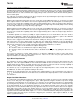
NOTES: A. C
L
includes probe and jig capacitance.
B. Waveform 1 is for an output with internal conditions such that the output is low, except when disabled by the output control.
Waveform 2 is for an output with internal conditions such that the output is high, except when disabled by the output control.
C. All input pulses are supplied by generators having the following characteristics: PRRv10 MHz, Z
O
= 50 Ω, dv/dt ≥ 1 V/ns.
D. The outputs are measured one at a time, with one transition per measurement.
E. t
PLZ
and t
PHZ
are the same as t
dis
.
F. t
PZL
and t
PZH
are the same as t
en
.
G. t
PLH
and t
PHL
are the same as t
pd
.
H. V
CCI
is the V
CC
associated with the input port.
I. V
CCO
is the V
CC
associated with the output port.
1.8 V ± 0.15 V
2.5 V ± 0.2 V
3.3 V ± 0.3 V
2 kΩ
2 kΩ
2 kΩ
V
CCO
R
L
0.15 V
0.15 V
0.3 V
V
TP
C
L
15 pF
15 pF
15 pF
TWL1200
www.ti.com
SCES786A –JUNE 2009–REVISED NOVEMBER 2009
PARAMETER MEASUREMENT INFORMATION
Figure 23. Push-Pull Buffered Direction Control Load Circuit and Voltage Waveform
Copyright © 2009, Texas Instruments Incorporated Submit Documentation Feedback 21
Product Folder Link(s): TWL1200