
Datasheet


TUSB7320, TUSB7340
SLLSE76E–MARCH 2011– REVISED JULY 2011
www.ti.com
Table 4-62. Link Control Register Description (continued)
Active State Link PM Control. This field is used to enable and disable
active state PM.
00 – Active State PM Disabled
1:0 ASLPMC rw
01 – L0s Entry Enabled
10 – L1 Entry Enabled
11 – L0s and L1 Entry Enable
4.44 Link Status Register
The Link Status Register indicates current state of the PCI Express Link.
PCI register offset: 82h
Register type:Read-only
Default value: 101xh
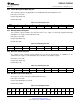
Table 4-63. PCI Register 82h
Bit
15 14 13 12 11 10 9 8 7 6 5 4 3 2 1 0
No.
Reset
0 0 0 1 0 0 0 0 0 0 0 1 0 0 x x
State
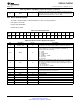
Table 4-64. Link Status Register Description
Bit Field Name Access Description
Link Autonomous Bandwidth Status. This bit has no function and is read
15 LINK_ABS r
only zero.
Link Bandwidth Management Status. This bit has no function and is read
14 LINK_BMS r
only zero.
13 DLL_ACTIVE r Data Link Layer Active. This bit has no function and is read only zero.
Slot Clock Configuration. This bit is ‘1’, since the TUSB73X0 uses the
12 SCC r
100-MHz differential reference clock provided by the platform.
11 LT r Link Training. This bit has no function and is read only zero.
10 TE r Retrain Link. This bit has no function and is read only zero.
Negotiated Link Width. This field is read only 000001b indicating the lane
9:4 NLW r
width is 1x.
3:0 LS r Link Speed. This field indicates the negotiated link speed.
4.45 Device Capabilities 2 Register
The Device Capabilities 2 Register indicates the device specific capabilities of the TUSB73X0.
PCI register offset: 94h
Register type:Read-only
Default value: 0000 0010h
50 CLASSIC PCI CONFIGURATION SPACE Copyright © 2011, Texas Instruments Incorporated
Submit Documentation Feedback
Product Folder Link(s): TUSB7320 TUSB7340