
Datasheet


TUSB7320, TUSB7340
www.ti.com
SLLSE76E–MARCH 2011– REVISED JULY 2011
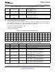
Table 4-99. PCI Register E0h
Bit
31 30 29 28 27 26 25 24 23 22 21 20 19 18 17 16
No.
Reset
0 0 0 0 0 0 0 0 0 0 0 0 0 0 0 0
State
Bit
15 14 13 12 11 10 9 8 7 6 5 4 3 2 1 0
No.
Reset
0 0 0 0 0 0 0 0 0 0 0 0 0 0 0 0
State
Table 4-100. USB Control Register Description
(1)(2)
Bit Field Name Access Description
USB Spread Spectrum Disable. When this bit is set to ‘1’, spread
31† USB_SPREAD_DIS† rw
spectrum generation for the USB 3.0 clock is disabled.
Frequency Select Enable. When this bit is set to 1, the oscillator is
restarted with the PLL multiplier value and the oscillator frequency
30* FREQ_SEL_EN* rw
controls set according to the value specified in the PLL_FREQ_SEL field.
This bit can only be written to once after power up.
PLL Frequency Select. If the FREQSEL pin is ‘1’, then the value in this
field controls the Frequency Select inputs to the PLL. In addition, the
frequency selector inputs to the Oscillator are set appropriately for the
frequency selected. If the FREQSEL pin is ‘0’, then this field has no
effect. Once the FREQ_SEL_EN bit has been set, this field will be locked
and cannot be changed.
000110 – 20 MHz xxxxxxxxxxxxxxx 010110 – 36 MHz
000111 – 21 MHz xxxxxxxxxxxxxxx 010111 – 37 MHz
001000 – 22 MHz xxxxxxxxxxxxxxx 011000 – 38 MHz
001001 – 23 MHz xxxxxxxxxxxxxxx 011001 – 38.4 MHz
001010 – 24 MHz xxxxxxxxxxxxxxx 011010 – 39 MHz
29:24* PLL_FREQ_SEL* rw 001011 – 25 MHz xxxxxxxxxxxxxxx 011011 – 40 MHz
001100 – 26 MHz xxxxxxxxxxxxxxx 011100 – 41 MHz
001101 – 27 MHz xxxxxxxxxxxxxxx 011101 – 42 MHz
001110 – 28 MHz xxxxxxxxxxxxxxx 011110 – 43 MHz
001111 – 29 MHz xxxxxxxxxxxxxxx 011111 – 44 MHz
010000 – 30 MHz xxxxxxxxxxxxxxx 100000 – 45 MHz
010001 – 31 MHz xxxxxxxxxxxxxxx 100001 – 46 MHz
010010 – 32 MHz xxxxxxxxxxxxxxx 100010 – 47 MHz
010011 – 33 MHz xxxxxxxxxxxxxxx 100011 – 48 MHz
010100 – 34 MHz xxxxxxxxxxxxxxx 100100 – 49 MHz
010101 – 35 MHz xxxxxxxxxxxxxxx 100101 – 50 MHz
All other values are reserved.
Hide MSI-X. When this bit is set, the Next Item Pointer Register (offset
23† HIDE_MSIX† rw 71h) for the PCI Express Capability is set to 00h, and BAR2 (offset 18h)
and BAR3 (offset 1Ch) are only zeros.
PWRONx Polarity. When this bit is ‘0’ (default), the PWRONx# pins are
active low and their internal pull-down resistors are enabled. When this
22* PWRON_POLARITY* rw
bit is ‘1’, the PWRONx# pins are active high and their internal pull-down
resistors are disabled.
21:17 RSVD r Reserved. Returns zero when read.
Port Power Control Not Present. When this bit is ‘0’, the TUSB73X0
forces the PPC bit to ‘1’ in the Host Controller Capability Parameters,
indicating that the system supports port power switches. When this bit is
16† PPC_NOT_PRESENT† rw
set to ‘1’, the TUSB73X0 forces the PPC bit to ‘0’ in the Host Controller
Capability Parameters, indicating that the system does not support port
power switches.
15:12† RSVD† rw Reserved. Returns zeros when read.
USB Port 4 Disable. When this bit is set to ‘1’, port 4 of the TUSB73X0 is
11† PORT4_DIS† rw disabled. For the TUSB7320 Port 4 is not present and this bit has no
effect.
(1) Bits marked with † are reset by a PCI Express reset (PERST#), a GRST#, or the internally-generated power-on reset
(2) Bits marked with * are reset by a GRST#
Copyright © 2011, Texas Instruments Incorporated CLASSIC PCI CONFIGURATION SPACE 61
Submit Documentation Feedback
Product Folder Link(s): TUSB7320 TUSB7340