
Datasheet


TUSB7320, TUSB7340
www.ti.com
SLLSE76E–MARCH 2011– REVISED JULY 2011
Table 4-94. General Control 0 Register Description
Bit Field Name Access Description
31:12 RSVD r Reserved. Returns zeros when read.
L1 Exit Latency for Asynchronous Clock. This value in this field is the
value reported in the L1_LATENCY field in the Link Capabilities Register
11:9† L1_EXIT_LAT_ASYNC† rw
when the CCC bit in the Link Control Register is ‘0’. This field defaults to
110b.
L1 Exit Latency for Common Clock. This value in this field is the value
8:6† L1_EXIT_LAT_COMMON† rw reported in the L1_LATENCY field in the Link Capabilities Register when
the CCC bit in the Link Control Register is ‘1’. This field defaults to 110b.
L0s Exit Latency for Asynchronous Clock. This value in this field is the
value reported in the L0s_LATENCY field in the Link Capabilities
5:3† L0s_EXIT_LAT_ASYNC† rw
Register when the CCC bit in the Link Control Register is ‘0’. This field
defaults to 011b.
L0s Exit Latency for Common Clock. This value in this field is the value
reported in the L0s_LATENCY field in the Link Capabilities Register
2:0† L0s_EXIT_LAT_COMMON† rw
when the CCC bit in the Link Control Register is ‘1’. This field defaults to
011b.
4.62 General Control 1 Register
This register is a read/write register is used to control various functions of the TUSB73X0. This register is
reset by a PCI Express reset (PERST#), a GRST#, or the internally-generated power-on reset.
PCI register offset: D8h
Register type:Read-Only,Read/Write
Default value: 0000 001Bh
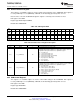
Table 4-95. PCI Register D8h
Bit
31 30 29 28 27 26 25 24 23 22 21 20 19 18 17 16
No.
Reset
0 0 0 0 0 0 0 0 0 0 0 0 0 0 0 0
State
Bit
15 14 13 12 11 10 9 8 7 6 5 4 3 2 1 0
No.
Reset
0 0 0 0 0 0 0 0 0 0 0 1 1 0 1 1
State
Table 4-96. General Control 1 Register Description
Bit Field Name Access Description
31:6 RSVD r Reserved. Returns zeros when read.
L1ASPM Entry Timer. This field specifies the value of the L1ASPM Entry
5:3† L1ASPM_ENTRY_TIMER† rw
Timer. This field defaults to ‘011’, corresponding to a value of 8 µs.
L0s Entry timer. This field specifies the value of the L0s Entry timer. This
2:0† L0s_ENTRY_TIMER† rw
field defaults to ‘011’, corresponding to a value of 4 µs.
Copyright © 2011, Texas Instruments Incorporated CLASSIC PCI CONFIGURATION SPACE 59
Submit Documentation Feedback
Product Folder Link(s): TUSB7320 TUSB7340