
Datasheet


TUSB2046B
TUSB2046BI
www.ti.com
SLLS413I –FEBRUARY 2000–REVISED SEPTEMBER 2013
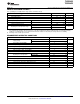
ABSOLUTE MAXIMUM RATINGS
(1)
over operating free-air temperature range (unless otherwise noted)
MIN MAX UNIT
V
CC
Supply voltage range
(2)
–0.5 3.6 V
V
I
Input voltage range –0.5 V
CC
+ 0.5 V
V
O
Output voltage range –0.5 V
CC
+ 0.5 V
I
IK
Input clamp current V
I
< 0 V or V
I
< V
CC
±20 mA
I
OK
Output clamp current V
O
< 0 V or V
O
< V
CC
±20 mA
T
stg
Storage temperature range –65 150 °C
TUSB2046B 0 70
T
A
Operating free-air temperature range °C
TUSB2046BI –40 85
(1) Stresses beyond those listed under “absolute maximum ratings” may cause permanent damage to the device. These are stress ratings
only, and functional operation of the device at these or any other conditions beyond those indicated under “recommended operating
conditions” is not implied. Exposure to absolute-maximum-rated conditions for extended periods may affect device reliability.
(2) All voltage levels are with respect to GND.
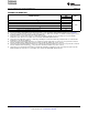
RECOMMENDED OPERATING CONDITIONS
PARAMETER MIN NOM MAX UNIT
TUSB2046B 3 3.3 3.6
V
CC
Supply voltage V
TUSB2046BI 3.3 3.6
V
I
Input voltage, TTL/LVCMOS 0 V
CC
V
V
O
Output voltage, TTL/LVCMOS 0 V
CC
V
V
IH(REC)
High-level input voltage, signal-ended receiver 2 V
CC
V
V
IL(REC)
Low-level input voltage, signal-ended receiver 0.8 V
V
IH(TTL)
High-level input voltage, TTL/LVCMOS 2 V
CC
V
V
IL(TTL)
Low-level input voltage, TTL/LVCMOS 0 0.8 V
TUSB2046B 0 70
T
A
Operating free-air temperature °C
TUSB2046BI –40 85
R
(DRV)
External series, differential driver resistor 22 (–5%) 22 (5%) Ω
f
(OPRH)
Operating (dc differential driver) high speed mode 12 Mb/s
f
(OPRL)
Operating (dc differential driver) low speed mode 1.5 Mb/s
V
ICR
Common mode, input range, differential receiver 0.8 2.5 V
t
t
Input transition times, TTL/LVCMOS 0 25 ns
T
J
Junction temperature range –40 115 °C
Copyright © 2000–2013, Texas Instruments Incorporated Submit Documentation Feedback 5
Product Folder Links: TUSB2046B TUSB2046BI