
Datasheet


(See Note A)
(See Note C)
(See Note B)
(See Note D)
TUSB1210
Link Controller
V
DDIO
V
BUS
V
BUS
EN
IN
5 V
OUT
V
BAT
V
DD33
C
VDD18
C
VDDIO
C
BYP
C
VDD33
C
VDD15
C
VBUS
V
DD18
V
DD15
7
27
5
13
12
17
4
10
V
BUS
Switch
USB Receptacle
ESD
3
9
29
6
2
31
GND
GND
1.8-V Supply
V
DDIO
Supply
3.1 5.5 V–
Supply
V
DDIO
Supply
CPEN
CS_OUT
DIR
STP
RESETB
CLOCK
CLOCK
NXT
DATA0
DATA1
DATA2
DATA3
DATA4
DATA5
DATA6
DATA7
DIR
STP
RESETB
REFCLK
NXT
DATA0
DATA1
DATA2
DATA3
DATA4
DATA5
DATA6
DATA7
1
20
21
22
26
N/C
25
N/C
24
N/C
16
N/C
15
N/C
8
32
28, 30
14
11
CS
CFG
18
23
19
DP
DM
ID
DP
DM
ID
SHIELD
(See Note E)
TUSB1210
www.ti.com
SLLSE09F –NOVEMBER 2009–REVISED AUGUST 2012
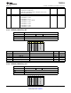
10 Application Information
10.1 Host or OTG, ULPI Input Clock Mode Application
Figure 10-1 shows a suggested application diagram for TUSB1210 in the case of ULPI input-clock mode
(60 MHz ULPI clock is provided by link processor), in Host or OTG application. Note this is just one
example, it is of course possible to operate as HOST or OTG while also in ULPI output-clock mode.
A. Pin 11 (CS) : can be tied high to VI
O
if CS_OUT pin unavailable; Pin 14 (CFG) : tie-high is Don’t Care since ULPI
clock is used in input mode
B. Pin 1 (REFCLK) : must be tied low
C. Ext 3 V supply supported
D. Pin 27 (RESETB) can be tied to V
DDIO
if unused.
E. Pins labeled N/C (no-connect) are truly no-connect, and can be tied or left floating.
Figure 10-1. Host or OTG, ULPI Input Clock Mode Application Diagram
10.2 Device, ULPI Output Clock Mode Application
Figure 10-2 shows a suggested application diagram for TUSB1210 in the case of ULPI output clock mode
(60 MHz ULPI clock is provided by TUSB1210, while link processor or another external circuit provides
REFCLK), in Device mode application. Note this is just one example, it is of course possible to operate as
Device while also in ULPI input-clock mode. Refer also to Figure 10-1.
Copyright © 2009–2012, Texas Instruments Incorporated Application Information 53
Submit Documentation Feedback
Product Folder Links: TUSB1210