
Datasheet


TUSB1210
www.ti.com
SLLSE09F –NOVEMBER 2009–REVISED AUGUST 2012
Table 6-4. TUSB1210 Modes vs ULPI Pin Status: USB Suspend Mode
(continued)
LINK / EXTERNAL RECOMMENDED
SUSPEND MODE
SETTING DURING SUSPEND MODE
PIN NO. PIN NAME DIR PU/PD DIR PU/PD
7 DATA4 O, (‘0’) - I -
9 DATA5 O, (‘0’) - I -
10 DATA6 O, (‘0’) - I -
13 DATA7 O, (‘0’) - I -
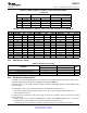
Table 6-5. TUSB1210 Modes vs ULPI Pin Status: ULPI 6-Pin Serial Mode and UART Mode
ULPI 6-PIN SERIAL MODE ULPI 3-PIN SERIAL MODE UART MODE
PIN NO. PIN NAME DIR PU/PD PIN NAME DIR PU/PD PIN NAME DIR PU/PD
26 CLOCK (1) IO - CLOCK (1) IO - CLOCK (1) IO -
31 DIR O - DIR O - DIR O -
2 NXT O - NXT O - NXT O -
29 STP I PU STP I PU STP I PU
3 TX_ENABLE I - TX_ENABLE I - TXD I -
4 TX_DAT I - DAT IO - RXD IO -
5 TX_SE0 I - SE0 IO - tie low O -
6 INT O - INT O - INT O -
7 RX_DP O - tie low O - tie low O -
9 RX_DM O - tie low O - tie low O -
10 RX_RCV O - tie low O - tie low O -
13 tie low O - tie low O - tie low O -
6.3.2 ULPI Interface Timing
Table 6-6. ULPI Interface Timing
INPUT CLOCK OUTPUT CLOCK
PARAMETER UNIT
MIN MAX MIN MAX
T
SC
,T
SD
Set-up time (control in, 8-bit data in) 3 6 ns
T
SC
,T
HD
Hold time (control in, 8-bit data in) 1.5 0 ns
T
DC
,T
DD
Output delay (control out, 8-bit data out) 6 9 ns
6.3.3 PHY Electrical Characteristics
The PHY is the physical signaling layer of the USB 2.0. It essentially contains all the drivers and receivers
required for physical data and protocol signaling on the DP and DM lines.
The PHY interfaces to the USB controller through a standard 12-pin digital interface called UTMI+ low pin
interface (ULPI).
The transmitters and receivers inside the PHY are classified into two main classes.
• The full-speed (FS) and low-speed (LS) transceivers. These are the legacy USB1.x transceivers.
• The HS (HS) transceivers
In order to bias the transistors and run the logic, the PHY also contains reference generation circuitry
which consists of:
• A DPLL which does a frequency multiplication to achieve the 480-MHz low-jitter lock necessary for
USB and also the clock required for the switched capacitor resistance block.
• A switched capacitor resistance block which is used to replicate an external resistor on chip.
Copyright © 2009–2012, Texas Instruments Incorporated USB Connectivity 19
Submit Documentation Feedback
Product Folder Links: TUSB1210