
Datasheet


www.ti.com
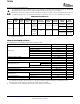
TIMING REQUIREMENTS for Figure 2 : I
2
C High-Speed Mode (f
SCL
= 1.7MHz)
(1)
TSC2004
SBAS408E – JUNE 2007 – REVISED MARCH 2008
All specifications typical at – 40 ° C to +85 ° C, SNSVDD = I/OVDD = +1.2V to +3.6V, unless otherwise noted.
2-WIRE HIGH-SPEED MODE PARAMETERS TEST CONDITIONS MIN MAX UNIT
SNSVDD ≥ 1.6V 10 µ s
Reset low time
(2)
t
WL(RESET)
1.2V ≤ SNSVDD < 1.6V 13 µ s
SCL clock frequency f
SCL
1.7 MHz
Hold time (repeated) START condition t
HD, STA
160 ns
Low period of SCL clock t
LOW
320 ns
High period of the SCL clock t
HIGH
120 ns
Setup time for a repeated START condition t
SU, STA
160 ns
Data hold time t
HD, DAT
0 150 ns
Data setup time t
SU, DAT
10 ns
Rise time of SCL signal t
RCL
C
b
= total bus capacitance 20 80 ns
Rise time of SDA signal t
RDA
C
b
= total bus capacitance 20 160 ns
Fall time of SCL signal t
FCL
C
b
= total bus capacitance 20 80 ns
Fall time of SDA signal t
FDA
C
b
= total bus capacitance 20 160 ns
Rise time of SCL signal after a repeated START
t
RCL1
C
b
= total bus capacitance 20 160 ns
condition and after an acknowledge bit
Setup time for STOP condition t
SU, STO
160 ns
Capacitive load for each bus line C
b
C
b
= total capacitance of one bus line in pF 400 pF
Pulse width of spike suppressed t
SP
0 10 ns
(1) All input signals are specified with t
R
= t
F
= 5ns (30% to 70% of V
DD
) and timed from a voltage level of (V
IL
+ V
IH
)/2.
(2) Refer to Figure 38 .
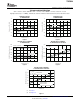
TIMING REQUIREMENTS for Figure 2 : I
2
C High-Speed Mode (f
SCL
= 3.4MHz)
(1)
All specifications typical at – 40 ° C to +85 ° C, SNSVDD = I/OVDD = +1.2V
(2)
to +3.6V, unless otherwise noted.
2-WIRE HIGH-SPEED MODE PARAMETERS TEST CONDITIONS MIN MAX UNIT
SNSVDD ≥ 1.6V 10 µ s
Reset low time
(3)
t
WL(RESET)
1.2V ≤ SNSVDD < 1.6V 13 µ s
SCL clock frequency f
SCL
3.4 MHz
Hold time (repeated) START condition t
HD, STA
160 ns
Low period of SCL clock t
LOW
160 ns
High period of the SCL clock t
HIGH
60 ns
Setup time for a repeated START condition t
SU, STA
160 ns
Data hold time t
HD, DAT
0 70 ns
Data setup time t
SU, DAT
10 ns
Rise time of SCL signal t
RCL
C
b
= total bus capacitance 10 40 ns
Rise time of SDA signal t
RDA
C
b
= total bus capacitance 10 80 ns
Fall time of SCL signal t
FCL
C
b
= total bus capacitance 10 40 ns
Fall time of SDA signal t
FDA
C
b
= total bus capacitance 10 80 ns
Rise time of SCL signal after a repeated START
t
RCL1
C
b
= total bus capacitance 10 80 ns
condition and after an acknowledge bit
Setup time for STOP condition t
SU, STO
160 ns
Capacitive load for each bus line C
b
C
b
= total capacitance of one bus line in pF 100 pF
Pulse width of spike suppressed t
SP
0 10 ns
(1) All input signals are specified with t
R
= t
F
= 5ns (30% to 70% of I/OVDD) and timed from a voltage level of (V
IL
+ V
IH
)/2.
(2) Because of the low supply voltage of 1.2V and the wide temperature range of – 40 ° C to +85 ° C, the I
2
C system devices may not reach
the maximum specification of I
2
C High-Speed mode, and f
SCL
may not reach 3.4Mhz.
(3) Refer to Figure 38 .
8 Submit Documentation Feedback Copyright © 2007 – 2008, Texas Instruments Incorporated
Product Folder Link(s): TSC2004