TS TSC2004 ® C20 04 SBAS408E – JUNE 2007 – REVISED MARCH 2008 1.2V to 3.6V, 12-Bit, Nanopower, 4-Wire TOUCH SCREEN CONTROLLER with I2C™ Interface FEATURES APPLICATIONS • • • • • • • • • • • 1 23 • • • • • • 4-Wire Touch Screen Interface Ratiometric Conversion Single 1.2V to 3.
TSC2004 www.ti.com SBAS408E – JUNE 2007 – REVISED MARCH 2008 This integrated circuit can be damaged by ESD. Texas Instruments recommends that all integrated circuits be handled with appropriate precautions. Failure to observe proper handling and installation procedures can cause damage. ESD damage can range from subtle performance degradation to complete device failure.
TSC2004 www.ti.com SBAS408E – JUNE 2007 – REVISED MARCH 2008 ELECTRICAL CHARACTERISTICS At TA = –40°C to +85°C, SNSVDD = VREF = +1.2V to +3.6V, I/OVDD (1) = +1.2V to +3.6V, unless otherwise noted.
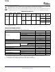
TSC2004 www.ti.com SBAS408E – JUNE 2007 – REVISED MARCH 2008 ELECTRICAL CHARACTERISTICS (continued) At TA = –40°C to +85°C, SNSVDD = VREF = +1.2V to +3.6V, I/OVDD = +1.2V to +3.6V, unless otherwise noted. TSC2004 PARAMETER TEST CONDITIONS MIN TYP MAX UNIT DIGITAL INPUT/OUTPUT Logic family CMOS VIH VIL Logic level 1.2V ≤ I/OVDD < 1.6V 0.7 × I/OVDD I/OVDD + 0.3 V 1.6V ≤ I/OVDD ≤ 3.6V 0.7 × I/OVDD I/OVDD + 0.3 V 1.2V ≤ I/OVDD < 1.6V –0.3 0.2 × I/OVDD V 1.6V ≤ I/OVDD ≤ 3.6V –0.3 0.
TSC2004 www.ti.
TSC2004 www.ti.com SBAS408E – JUNE 2007 – REVISED MARCH 2008 TIMING INFORMATION S Sr P S SDA tSU, STA tSU, DAT tBUF tHD, STA tHD, DAT tLOW SCL tSU, STO tHIGH tHD, STA tR tF S = START Condition Sr = Repeated START Condition P = STOP Condition = Resistor Pull-Up Figure 1.
TSC2004 www.ti.com SBAS408E – JUNE 2007 – REVISED MARCH 2008 TIMING REQUIREMENTS for Figure 1: I2C Standard Mode (fSCL = 100kHz) (1) All specifications typical at –40°C to +85°C, SNSVDD = I/OVDD = +1.2V to +3.6V, unless otherwise noted.
TSC2004 www.ti.com SBAS408E – JUNE 2007 – REVISED MARCH 2008 TIMING REQUIREMENTS for Figure 2: I2C High-Speed Mode (fSCL = 1.7MHz) (1) All specifications typical at –40°C to +85°C, SNSVDD = I/OVDD = +1.2V to +3.6V, unless otherwise noted. 2-WIRE HIGH-SPEED MODE PARAMETERS Reset low time (2) TEST CONDITIONS tWL(RESET) MIN SNSVDD ≥ 1.6V 10 1.2V ≤ SNSVDD < 1.
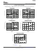
TSC2004 www.ti.com SBAS408E – JUNE 2007 – REVISED MARCH 2008 TYPICAL CHARACTERISTICS At TA = –40°C to +85°C, SNSVDD = VREF = +1.2V to +3.6V, I/OVDD = +1.2V to +3.6V, fADC = fOSC/2, High-Speed mode (fSCL = 3.4MHz), 12-bit mode, and non-continuous AUX measurement, unless otherwise noted. CHANGE IN OFFSET vs TEMPERATURE CHANGE IN GAIN vs TEMPERATURE 1.5 1.5 SNSVDD = IOVDD = VREF SNSVDD = I/OVDD = VREF 1.0 Delta from +25°C (LSB) Delta from +25°C (LSB) 1.0 0.5 SNSVDD = 1.6V 0 SNSVDD = 3.0V -0.
TSC2004 www.ti.com SBAS408E – JUNE 2007 – REVISED MARCH 2008 TYPICAL CHARACTERISTICS (continued) At TA = –40°C to +85°C, SNSVDD = VREF = +1.2V to +3.6V, I/OVDD = +1.2V to +3.6V, fADC = fOSC/2, High-Speed mode (fSCL = 3.4MHz), 12-bit mode, and non-continuous AUX measurement, unless otherwise noted. POWER-DOWN SUPPLY CURRENT vs TEMPERATURE POWER-DOWN SUPPLY CURRENT vs SNSVDD SUPPLY VOLTAGE 60 SNSVDD = I/OVDD = VREF Power-Down Supply Current (nA) Power-Down Supply Current (nA) 1000 800 SNSVDD = 3.
TSC2004 www.ti.com SBAS408E – JUNE 2007 – REVISED MARCH 2008 TYPICAL CHARACTERISTICS (continued) At TA = –40°C to +85°C, SNSVDD = VREF = +1.2V to +3.6V, I/OVDD = +1.2V to +3.6V, fADC = fOSC/2, High-Speed mode (fSCL = 3.4MHz), 12-bit mode, and non-continuous AUX measurement, unless otherwise noted.
TSC2004 www.ti.com SBAS408E – JUNE 2007 – REVISED MARCH 2008 TYPICAL CHARACTERISTICS (continued) At TA = –40°C to +85°C, SNSVDD = VREF = +1.2V to +3.6V, I/OVDD = +1.2V to +3.6V, fADC = fOSC/2, High-Speed mode (fSCL = 3.4MHz), 12-bit mode, and non-continuous AUX measurement, unless otherwise noted. INTERNAL OSCILLATOR CLOCK FREQUENCY vs TEMPERATURE INTERNAL OSCILLATOR CLOCK FREQUENCY vs TEMPERATURE 3.90 SNSVDD = I/OVDD = VREF = 3.0V Internal Clock Frequency (MHz) Internal Clock Frequency (MHz) 4.
TSC2004 www.ti.com SBAS408E – JUNE 2007 – REVISED MARCH 2008 OVERVIEW The TSC2004 is an analog interface circuit for a human interface touch screen device. A register-based architecture eases integration with microprocessor-based systems through a standard I2C bus. All peripheral functions are controlled through the registers and onboard state machines.
TSC2004 www.ti.com SBAS408E – JUNE 2007 – REVISED MARCH 2008 1.6VDC 1 mF 1 mF 1m F 0.1mF 0.1mF AGND 0.1mF 1.6VDC VREF 1.2kW I/OVDD X+ SNSVDD DGND SNSGND 1.2kW PINTDAV GPIO RESET GPIO Y+ SDA TSC2004 X- SDA Auxilary Input AD1 AD0 DGND SUBGND AUX AGND Y- SNSGND SCL Touch Screen Host Processor SCL (PINTDAV is optional; software implementation polling of the Status register is possible) AGND Figure 24.
TSC2004 www.ti.com SBAS408E – JUNE 2007 – REVISED MARCH 2008 The A/D converter converts the voltage measured at the point where the panel is touched. A measurement of the Y position of the pointing device is made by connecting the X+ input to a data converter chip, turning on the Y+ and Y– drivers, and digitizing the voltage seen at the X+ input. The voltage measured is determined by the voltage divider developed at the point of touch.
TSC2004 www.ti.com SBAS408E – JUNE 2007 – REVISED MARCH 2008 When the touch panel is pressed or touched and the drivers to the panel are turned on, the voltage across the touch panel often overshoots and then slowly settles down (decays) to a stable dc value. This effect is a result of mechanical bouncing caused by vibration of the top layer sheet of the touch panel when the panel is pressed. This settling time must be accounted for, or else the converted value will be in error.
TSC2004 www.ti.com SBAS408E – JUNE 2007 – REVISED MARCH 2008 INTERNAL TEMPERATURE SENSOR In some applications, such as battery recharging, an ambient temperature measurement is required. The temperature measurement technique used in the TSC2004 relies on the characteristics of a semiconductor junction operating at a fixed current level. The forward diode voltage (VBE) has a well-defined characteristic versus temperature.
TSC2004 www.ti.com SBAS408E – JUNE 2007 – REVISED MARCH 2008 ANALOG-TO-DIGITAL CONVERTER Figure 28 shows the analog inputs of the TSC2004. The analog inputs (X, Y, and Z touch panel coordinates, chip temperature and auxiliary inputs) are provided via a multiplexer to the Successive Approximation Register (SAR) Analog-to-Digital (A/D) converter. The A/D architecture is based on capacitive redistribution architecture, which inherently includes a sample-and-hold function.
TSC2004 www.ti.com SBAS408E – JUNE 2007 – REVISED MARCH 2008 Data Format The TSC2004 output data are in Straight Binary format as shown in Figure 29. This figure shows the ideal output code for the given input voltage and does not include the effects of offset, gain, or noise. FS = Full-Scale Voltage = VREF(1) 1LSB = VREF(1)/4096 1LSB 11...111 Output Code 11...110 11...101 00...010 00...001 00...000 0V Input Voltage (2) FS - 1LSB (V) (1) Reference voltage at converter: +REF – (–REF).
TSC2004 www.ti.com SBAS408E – JUNE 2007 – REVISED MARCH 2008 Touch Detect PINTDAV can be programmed to generate an interrupt to the host. Figure 30 details an example for the Y-position measurement. While in the power-down mode, the Y– driver is on and connected to GND. The internal pen-touch signal depends on whether or not the X+ input is driven low.
TSC2004 www.ti.com SBAS408E – JUNE 2007 – REVISED MARCH 2008 Preprocessing The TSC2004 offers an array of powerful preprocessing operations that reduce unnecessary traffic on the bus and reduce the host processor loading. This reduction is especially critical for the serial interface, where limited bandwidth is a tradeoff, keeping the connection lines to a minimum. All data acquisition tasks are looking for specific data that meet certain criteria.
TSC2004 www.ti.com SBAS408E – JUNE 2007 – REVISED MARCH 2008 NOTE: The default setting for MAVF is MVF (median value filter with averaging bypassed) for any invalid configuration. For example, if (M1, M0, W1, W0) = (1,0,1,0), the MAVF performs as it was configured for (1,0,0,0), median filter only with filter size = 7 and no averaging. The only exception is M > 1 and (W1, W0) = (1,1). This setting is reserved and should not be used. Table 3.
TSC2004 www.ti.com SBAS408E – JUNE 2007 – REVISED MARCH 2008 I2C INTERFACE The TSC2004 supports the I2C serial bus and data transmission protocol in all three defined modes: standard, fast, and high-speed. A device that sends data onto the bus is defined as a transmitter, and a device receiving data as a receiver. The device that controls the message is called a master. Devices controlled by the master are slaves.
TSC2004 www.ti.com SBAS408E – JUNE 2007 – REVISED MARCH 2008 Figure 32 details how data transfer is accomplished on the I2C bus. Depending upon the state of the R/W bit, two types of data transfer are possible: 1. Data transfer from a master transmitter to a slave receiver. The first byte transmitted by the master is the slave address. Next follows a number of data bytes. The slave returns an acknowledge bit after the slave address and each received byte. 2.
TSC2004 www.ti.com SBAS408E – JUNE 2007 – REVISED MARCH 2008 I2C High-Speed Mode (Hs Mode) Serial data transfer format in High-Speed (Hs) mode meets the Fast or Standard (F/S) mode I2C bus specification. Hs mode can only commence after the following conditions (all of which are in F/S mode) exist: 1. START condition (S) 2. 8-bit master code (00001xxx) 3. not-acknowledge bit (N) Figure 33 shows this sequence in more detail.
TSC2004 www.ti.com SBAS408E – JUNE 2007 – REVISED MARCH 2008 DIGITAL INTERFACE ADDRESS BYTE The TSC2004 has a 7-bit slave address word. The first five bits (MSBs) of the slave address are factory-preset to comply with the I2C standard for A/D converters and are always set at '10010'. The logic state of the address input pins (AD1-AD0) determine the two LSBs of the device address to activate communication.
TSC2004 www.ti.com SBAS408E – JUNE 2007 – REVISED MARCH 2008 Table 6. Control Byte 1 Bit Register Description (D7 = 1) BIT NAME D7 Control Byte ID D6-D3 C3:C0 D2 RM D1 SWRST D0 STS DESCRIPTION 1 Converter Function Select as detailed in Table 7 0: 10 Bit 1: 12 Bit Software Reset. This bit is self-clearing. 1: Reset all register values to default Stop bit for all converter functions. This bit is self-clearing.
TSC2004 www.ti.com SBAS408E – JUNE 2007 – REVISED MARCH 2008 Touch Screen Scan Function for XYZ or XY C3-C0 = 0000 or 0001: These scan functions can collaborate with the PSM bit that defines the control mode of converter functions. If the PSM bit is set to '1', these scan function select commands are recommended to be issued before a pen touch is detected in order to allow the TSC2004 to initiate and control the scan processes immediately after the screen is touched.
TSC2004 www.ti.com SBAS408E – JUNE 2007 – REVISED MARCH 2008 Table 9.
TSC2004 www.ti.com SBAS408E – JUNE 2007 – REVISED MARCH 2008 START A WRITE CYCLE A write cycle begins when the master issues the slave address to the TSC2004. The slave address consists of seven address bits and a write bit (R/W = 0; see Table 5). When the eighth bit has been received and the address matches the AD1-AD0 address input pin setting, the TSC2004 issues an acknowledge bit by pulling SDA low for one additional clock cycle (ACK = 0); see Figure 34.
TSC2004 www.ti.com SBAS408E – JUNE 2007 – REVISED MARCH 2008 REGISTER ACCESS Data access begins with the master issuing a START (or repeated START) condition followed by the 7-bit address and a read bit (R/W = 1; see Table 5). When the eighth bit has been received and the address matches, the slave issues an acknowledge by pulling SDA low for one clock cycle (ACK = 0). The first byte of serial data then follows.
TSC2004 www.ti.
TSC2004 www.ti.com SBAS408E – JUNE 2007 – REVISED MARCH 2008 COMMUNICATION PROTOCOL The TSC2004 is controlled entirely by registers. Reading and writing to these registers are accomplished by the use of Control Byte 0, which includes a 4-bit address plus one read/write TSC register control bit. The data registers defined in Table 10 are all 16-bit, right-adjusted.
TSC2004 www.ti.com SBAS408E – JUNE 2007 – REVISED MARCH 2008 CL1, CL0—Conversion clock control. These two bits specify the clock rate that the A/D converter uses to perform conversion, as shown in Table 15. Table 15. A/D Converter Conversion Clock Control (1) CL1 CL0 FUNCTION 0 0 fADC = fOSC/1. This is referred to as the 4MHz A/D converter clock rate, 10-bit resolution only (1). 0 1 fADC = fOSC/2. This is referred to as the 2MHz A/D converter clock rate. 1 0 fADC = fOSC/4.
TSC2004 www.ti.com SBAS408E – JUNE 2007 – REVISED MARCH 2008 Table 18. Sense Time Selection SNS2 SNS1 SNS0 SENSE TIME (tSNS) 0 0 0 32µs 0 0 1 96µs 0 1 0 544µs 0 1 1 608µs 1 0 0 2.080ms 1 0 1 2.144ms 1 1 0 2.592ms 1 1 1 2.656ms DTW—Detection of pen touch in wait (patent pending). Writing a '1' to this bit enables the pen touch detection in the background while waiting for the host to issue the converter function in host-initiated/controlled modes.
TSC2004 www.ti.com SBAS408E – JUNE 2007 – REVISED MARCH 2008 BTD2-BTD0—Batch Time Delay mode. These are the selection bits that specify the delay before a sample/conversion scan cycle is triggered. When it is set, Batch Time Delay mode uses a set of timers to automatically trigger a sequence of sample-and-conversion events. The mode works for both TSC-initiated scans (XYZ or XY) and host-initiated scans (XYZ or XY).
TSC2004 www.ti.com SBAS408E – JUNE 2007 – REVISED MARCH 2008 Configuration Register 2 Configuration register 2 (CFR2) defines the preprocessor configuration. Table 22. Configuration Register 2 (Reset Value = 0000h) MSB D15 D14 D13 D12 D11 D10 D9 D8 D7 D6 D5 D4 D3 D2 D1 LSB D0 PINTS1 PINTS0 M1 M0 W1 W0 TZ1 TZ0 AZ1 AZ0 Resrvd MAVE X MAVE Y MAVE Z MAVE AUX MAVE TEMP PINTS1 (default 0)—This bit controls the output format of the PINTDAV pin.
TSC2004 www.ti.com SBAS408E – JUNE 2007 – REVISED MARCH 2008 Converter Function Select Register The Converter Function Select (CFN) register reflects the converter function select status. Table 25. Converter Function Select Status Register (Reset Value = 0000h) MSB D15 D14 D13 D12 D11 D9 D8 D7 D6 D5 D4 D3 D2 D1 LSB D0 CFN9 CFN8 CFN7 CFN6 CFN5 CFN4 CFN3 CFN2 CFN1 CFN0 D10 CFN15 CFN14 CFN13 CFN12 CFN11 CFN10 CFN15-CFN13—Touch screen drivers status.
TSC2004 www.ti.com SBAS408E – JUNE 2007 – REVISED MARCH 2008 PDST—Power down status. This bit reflects the setting of the PND0 bit in Control Byte 0. When this bit shows '0', it indicates A/D converter bias circuitry is still powered on after each conversion and before the next sampling; otherwise, it indicates A/D converter bias circuitry is powered down after each conversion and before the next sampling. However, it is powered down between conversion sets.
TSC2004 www.ti.com SBAS408E – JUNE 2007 – REVISED MARCH 2008 REGISTER RESET There are three way to reset the TSC2004. First, at power-on, a power good signal generates a prolonged reset pulse internally to all registers. Second, an external pin, RESET, is available to perform a system reset or allow other peripherals (such as a display) to reset the device if the pulse meets the timing requirement (at least 10µs wide). Any RESET pulse less than 5µs will be rejected.
TSC2004 www.ti.com SBAS408E – JUNE 2007 – REVISED MARCH 2008 THEORY OF OPERATION TOUCH SCREEN MEASUREMENTS As noted previously in the discussion of the A/D converter, several operating modes can be used that allow great flexibility for the host processor. This section examines these different modes. Conversion Controlled by TSC2004 Initiated by TSC2004 (TSMode 1) In TSMode 1, before a pen touch can be detected, the TSC2004 must be programmed with PSM = 1 and one of two scan modes: 1.
TSC2004 www.ti.com SBAS408E – JUNE 2007 – REVISED MARCH 2008 Table 31.
TSC2004 www.ti.com SBAS408E – JUNE 2007 – REVISED MARCH 2008 If the pressure of the touch is also to be measured, the process continues in the same way, but measuring the Z1 and Z2 values instead, and storing the results in temporary registers. Once the complete sample set of data (X, Y, Z1, and Z2) are available, they are loaded in the X, Y, Z1, and Z2 registers. This process is illustrated in Figure 40. As before, this process time depends upon the settings described above.
TSC2004 www.ti.com SBAS408E – JUNE 2007 – REVISED MARCH 2008 Conversion Controlled by TSC2004 Initiated by Host (TSMode 2) In TSMode 2, the TSC2004 detects when the touch panel is touched and causes the internal Pen-Touch signal to activate, which lowers the PINTDAV output if it is programmed as PENIRQ. The host recognizes the interrupt request, and then writes to the A/D Converter Control register to select one of the two touch screen scan functions: 1.
TSC2004 www.ti.com SBAS408E – JUNE 2007 – REVISED MARCH 2008 Conversion Controlled by Host (TSMode 3) In TSMode 3, the TSC2004 detects when the touch panel is touched and causes the internal Pen-Touch signal to be active, which lowers the PINTDAV output if it is programmed as PENIRQ. The host recognizes the interrupt request. Instead of starting a sequence in the TSC2004, which then reads each coordinate in turn, the host must now control all aspects of the conversion.
TSC2004 www.ti.
TSC2004 www.ti.
TSC2004 www.ti.com SBAS408E – JUNE 2007 – REVISED MARCH 2008 AUXILIARY AND TEMPERATURE MEASUREMENT The TSC2004 can measure the voltage from the auxiliary input (AUX) and from the internal temperature sensor. Applications for the AUX can include external temperature sensing, ambient light monitoring for controlling backlighting, or sensing the current drawn from batteries. There are two converter functions that can be used for the measurement of the AUX: 1.
TSC2004 www.ti.com SBAS408E – JUNE 2007 – REVISED MARCH 2008 LAYOUT The following layout suggestions should obtain optimum performance from the TSC2004. However, many portable applications have conflicting requirements for power, cost, size, and weight. In general, most portable devices have fairly clean power and grounds because most of the internal components are very low power. This situation would mean less bypassing for the converter power and less concern regarding grounding.
TSC2004 www.ti.com SBAS408E – JUNE 2007 – REVISED MARCH 2008 Revision History NOTE: Page numbers for previous revisions may differ from page numbers in the current version. Changes from Revision D (February 2008) to Revision E ............................................................................................. Page • • • • • • Changed air gap discharge from 18kV to 25kV in the ESD protection discharge sub-bullets of Features ...........................
PACKAGE OPTION ADDENDUM www.ti.
PACKAGE OPTION ADDENDUM www.ti.com 11-Apr-2013 Important Information and Disclaimer:The information provided on this page represents TI's knowledge and belief as of the date that it is provided. TI bases its knowledge and belief on information provided by third parties, and makes no representation or warranty as to the accuracy of such information. Efforts are underway to better integrate information from third parties.
PACKAGE MATERIALS INFORMATION www.ti.com 14-Jul-2012 TAPE AND REEL INFORMATION *All dimensions are nominal Device TSC2004IRTJR Package Package Pins Type Drawing QFN RTJ 20 SPQ Reel Reel A0 Diameter Width (mm) (mm) W1 (mm) B0 (mm) K0 (mm) P1 (mm) W Pin1 (mm) Quadrant 3000 330.0 12.4 4.25 4.25 1.15 8.0 12.0 Q2 TSC2004IRTJT QFN RTJ 20 250 180.0 12.4 4.25 4.25 1.15 8.0 12.0 Q2 TSC2004IYZKR DSBGA YZK 24 3000 180.0 8.4 2.75 2.75 0.81 4.0 8.
PACKAGE MATERIALS INFORMATION www.ti.com 14-Jul-2012 *All dimensions are nominal Device Package Type Package Drawing Pins SPQ Length (mm) Width (mm) Height (mm) TSC2004IRTJR QFN RTJ 20 3000 367.0 367.0 35.0 TSC2004IRTJT QFN RTJ 20 250 210.0 185.0 35.0 TSC2004IYZKR DSBGA YZK 24 3000 210.0 185.0 35.0 TSC2004IYZKR DSBGA YZK 24 3000 217.0 193.0 35.0 TSC2004IYZKT DSBGA YZK 24 250 210.0 185.0 35.0 TSC2004IYZKT DSBGA YZK 24 250 217.0 193.0 35.
D: Max = 2.598 mm, Min =2.538 mm E: Max = 2.598 mm, Min =2.
IMPORTANT NOTICE Texas Instruments Incorporated and its subsidiaries (TI) reserve the right to make corrections, enhancements, improvements and other changes to its semiconductor products and services per JESD46, latest issue, and to discontinue any product or service per JESD48, latest issue. Buyers should obtain the latest relevant information before placing orders and should verify that such information is current and complete.