
Datasheet


TSC2003
6
SBAS162G
www.ti.com
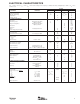
POWER-ON SEQUENCE TIMING
POWER-ON SEQUENCE TIMING DIAGRAM
During TSC2003 power-up, the I
2
C bus should be idle. In
other words, the SDA and SCL lines must be high before the
TSC supply (+VDD) ramps up greater than 0.9V. If the TSC
uses the same supply as the the I
2
C bus pull-up resistors
(V
I2C
), then a 1µF capacitor placed very close to the TSC
supply pin will cause the TSC supply to ramp up more slowly
(refer to the Power-On Sequence timing diagram). If the TSC
supply (+VDD) is different than the supply to the I
2
C bus pull-
up resistors (V
I2C
), then V
I2C
should be turned on before the
TSC supply (+VDD) is powered up.
TSC Supply
+VDD
100% V
DD
~ 0.9V
t
1
≥ 0
0V
~ 0.9V
0V
~ 0.9V
0V
SCL
SDA
SCL High
SDA Low
I
2
C Bus Activity
I
2
C Bus Activity
100% V
I2C
100% V
I2C