
Datasheet


2–10
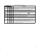
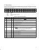
Table 2–8. Physical Layer Terminals
TERMINAL
NAME PDT
NO.
PGE
NO.
TYPE I/O DESCRIPTION
CNA 67 77 CMOS I/O
Cable not active. This terminal is asserted high when there are no ports receiving incoming
bias voltage. If not used, this terminal must be strapped either to DV
DD
or to GND through
a resistor. To enable the CNA terminal, the BIOS must set bit 7 (CNAOUT) of the PCI PHY
control register at offset ECh in the PCI configuration space (see Section 3.20, PCI PHY
Control Register). If an EEPROM is implemented and CNA functionality is needed, bit 7 of
byte offset 16h in the serial EEPROM must be set. This sets the bit in the PCI configuration
space at power up via the EEPROM.
CPS 69 79 CMOS I
Cable power status input. This terminal is normally connected to cable power through a
400-kΩ resistor. This circuit drives an internal comparator that detects the presence of cable
power. If CPS does not detect cable power, this terminal must be pulled to AV
DD
.
FILTER0
FILTER1
101
102
115
116
CMOS I/O
PLL filter terminals. These terminals are connected to an external capacitance to form a
lag-lead filter required for stable operation of the internal frequency multiplier PLL running
off of the crystal oscillator. A 0.1-µF ±10% capacitor is the only external component required
to complete this filter.
PC0
PC1
PC2
64
63
62
70
69
68
CMOS I
Power class programming inputs. On hardware reset, these inputs set the default value of
the power class indicated during self-ID. Programming is done by tying these terminals high
or low.
R0
R1
100
99
114
113
Bias –
Current-setting resistor terminals. These terminals are connected to an external resistance
to set the internal operating currents and cable driver output currents. A resistance of
6.34 kΩ ±1% is required to meet the IEEE Std 1394-1995 output voltage limits.
TPA0+
TPA0–
78
77
88
87
Cable I/O
TPA1+
TPA1–
87
86
97
96
Cable I/O
Twisted-pair cable A differential signal terminals. Board trace lengths from each pair of
positive and negative differential signal pins must be matched and as short as possible to
the external load resistors and to the cable connector
TPA2+
TPA2–
95
94
105
104
Cable I/O
th
e ex
t
erna
l
l
oa
d
res
i
s
t
ors an
d
t
o
th
e ca
bl
e connec
t
or.
TPB0+
TPB0–
75
74
85
84
Cable I/O
TPB1+
TPB1–
83
82
93
92
Cable I/O
Twisted-pair cable B differential signal terminals. Board trace lengths from each pair of
positive and negative differential signal pins must be matched and as short as possible to
the external load resistors and to the cable connector
TPB2+
TPB2–
92
91
102
101
Cable I/O
th
e ex
t
erna
l
l
oa
d
res
i
s
t
ors an
d
t
o
th
e ca
bl
e connec
t
or.
TPBIAS0
TPBIAS1
TPBIAS2
79
88
96
89
98
106
Cable I/O
Twisted-pair bias output. This provides the 1.86-V nominal bias voltage needed for proper
operation of the twisted-pair cable drivers and receivers and for signaling to the remote
nodes that there is an active cable connection. Each of these pins must be decoupled with
a 1.0-µF capacitor to ground.
XI
XO
105
106
119
120
Crystal –
Crystal oscillator inputs. These pins connect to a 24.576-MHz parallel resonant fundamental
mode crystal. The optimum values for the external shunt capacitors are dependent on the
specifications of the crystal used (see Section 8.2, Crystal Selection). Terminal 5 has an
internal 10-kΩ (nominal value) pulldown resistor. An external clock input can be connected
to the XI terminal. When using an external clock input, the XO terminal must be left
unconnected. Refer to Section 9.7 for the operating characteristics of the XI terminal.