
Datasheet


Crystal Selection
C
L
+
C9 C10
C9 ) C10
) C
PHY
) C
BD
TSB41BA3D
www.ti.com
............................................................................................................................................... SLLS959A – DECEMBER 2008 – REVISED MARCH 2009
The TSB41BA3D and other Texas Instruments PHY devices are designed to use an external 49.152-MHz crystal
connected between the XI and XO terminals to provide the reference for an internal oscillator circuit. This
oscillator in turn drives a PLL circuit that generates the various clocks required for transmission and
resynchronization of data at the S100 through S400 media data rates.
A variation of less than ± 100 ppm from nominal for the media data rates is required by IEEE Std 1394. Adjacent
PHYs can therefore have a difference of up to 200 ppm from each other in their internal clocks, and PHYs must
be able to compensate for this difference over the maximum packet length. Larger clock variations can cause
resynchronization overflows or underflows, resulting in corrupted packet data or even PHY lockup.
For the TSB41BA3D, the PCLK output can be used to measure the frequency accuracy and stability of the
internal oscillator and PLL from which it is derived. When operating the PHY-LLC interface with a non-1394b
LLC, the frequency of the PCLK output must be within ± 100 ppm of the nominal frequency of 49.152 MHz. When
operating the PHY-LLC interface with a 1394b LLC, the frequency of the PCLK output must be within ± 100 ppm
of the nominal frequency of 98.304 MHz.
The following are some typical specifications for crystals used with the physical layers from Texas Instruments in
order to achieve the required frequency accuracy and stability:
• Crystal mode of operation: Fundamental
• Frequency tolerance at 25 ° C: Total frequency variation for the complete circuit is ± 100 ppm. A crystal with
± 30 ppm frequency tolerance is recommended for adequate margin.
• Frequency stability (over temperature and age): A crystal with ± 30 ppm frequency stability is recommended
for adequate margin.
NOTE:
The total frequency variation must be kept below ± 100 ppm from nominal with some
allowance for error introduced by board and device variations. Trade-offs between
frequency tolerance and stability can be made as long as the total frequency variation
is less than ± 100 ppm. For example, the frequency tolerance of the crystal can be
specified at 50 ppm, and the temperature tolerance can be specified at 30 ppm to
give a total of 80 ppm possible variation due to the oscillator alone. Aging also
contributes to the frequency variation.
• Load capacitance: For parallel resonant mode crystal circuits, the frequency of oscillation depends on the
load capacitance specified for the crystal. Total load capacitance (C
L
) is a function of not only the discrete
load capacitors, but also board layout and circuit. It might be necessary to select discrete load capacitors
iteratively until the PCLK output is within specification. It is recommended that load capacitors with a
maximum of ± 5% tolerance be used.
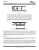
As an example, for the OHCI + 41LV03 evaluation module (EVM), which uses a crystal specified for 12-pF
loading, load capacitors (C9 and C10 in Figure 10 ) of 16 pF each were appropriate for the layout of that
particular board. The load specified for the crystal includes the load capacitors (C9, C10), the loading of the PHY
terminals (C
PHY
), and the loading of the board itself (C
BD
). The value of C
PHY
is typically about 1 pF and C
BD
is
typically 0.8 pF per centimeter of board etch; a typical board can have 3 pF to 6 pF or more. The load capacitors
C9 and C10 combine as capacitors in series so that the total load capacitance is:
Copyright © 2008 – 2009, Texas Instruments Incorporated Submit Documentation Feedback 29
Product Folder Link(s): TSB41BA3D