
Datasheet


V
+
GND
NC or NO
V
NC
or V
NO
V
I
NC or NO
COM
V
COM
C
L
(2)
R
L
t
BBM
50%
90% 90%
V
NC
or V
NO
= V
+
R
L
= 50 Ω
C
L
= 35 pF
Logic
Input
(1)
Logic
Input
(V
I
)
Switch
Output
(V
COM
)
V
+
0
IN
V
+
GND
NC
V
I
NO
COM
50 W
50 W
V
NC
V
COM
Channel ON: NC to COM
Network Analyzer Setup
Source Power = 0 dBm
(632-mV P-P at 50-W load)
DC Bias = 350 mV
Network Analyzer
Source
Signal
+
V
I
= V
+
or GND
IN
TS5A9411
SCDS241A – MAY 2008 – REVISED JULY 2008 ...............................................................................................................................................................
www.ti.com
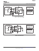
A. All input pulses are supplied by generators having the following characteristics: PRR ≤ 10 MHz, Z
O
= 50 Ω , t
r
< 5 ns,
t
f
< 5 ns.
B. C
L
includes probe and jig capacitance.
Figure 11. Break-Before-Make Time (t
BBM
)
Figure 12. Bandwidth (BW)
14 Submit Documentation Feedback Copyright © 2008, Texas Instruments Incorporated
Product Folder Link(s): TS5A9411