
Datasheet


TS5A9411
SCDS241A – MAY 2008 – REVISED JULY 2008 ...............................................................................................................................................................
www.ti.com
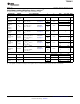
PIN DESCRIPTION
PIN
NAME DESCRIPTION
NO.
1 IN Digital control to connect COM to NO
2 V
+
Power supply
3 GND Digital ground
4 NC Normally closed
5 COM Common
6 NO Normally open
PARAMETER DESCRIPTION
SYMBOL DESCRIPTION
V
COM
Voltage at COM
V
NC
Voltage at NC
V
NO
Voltage at NO
r
ON
Resistance between COM and NC or COM and NO ports when the channel is ON
Δ r
ON
Difference of r
on
between channels
r
ON(flat)
Difference between the maximum and minimum value of r
on
in a channel over the specified range of conditions
Leakage current measured at the NC port, with the corresponding channel (NC to COM) in the OFF state under
I
NC(OFF)
worst-case input and output conditions
Leakage current measured at the NO port, with the corresponding channel (NO to COM) in the OFF state under
I
NO(OFF)
worst-case input and output conditions
Leakage current measured at the NC port, with the corresponding channel (NC to COM) in the ON state and the
I
NC(ON)
output (COM) being open
Leakage current measured at the NO port, with the corresponding channel (NO to COM) in the ON state and the
I
NO(ON)
output (COM) being open
Leakage current measured at the COM port, with the corresponding channel (COM to NO or COM to NC) in the ON
I
COM(ON)
state and the output (NC or NO) being open
I
COM(PWROFF)
Leakage current measured at the COM port during the power-down condition, V
+
= 0
V
IH
Minimum input voltage for logic high for the control input (IN)
V
IL
Maximum input voltage for logic low for the control input (IN)
V
I
Voltage at IN
I
IH
, I
IL
Leakage current measured at IN
Turn-on time for the switch. This parameter is measured under the specified range of conditions and by the
t
ON
propagation delay between the digital control (IN) signal and analog outputs (COM, NC, or NO) signal when the
switch is turning ON.
Turn-off time for the switch. This parameter is measured under the specified range of conditions and by the
t
OFF
propagation delay between the digital control (IN) signal and analog outputs (COM, NC, or NO) signal when the
switch is turning OFF.
Break-before-make time. This parameter is measured under the specified range of conditions and by the
t
BBM
propagation delay between the output of two adjacent analog channels (NC and NO) when the control signal
changes state.
Charge injection is a measurement of unwanted signal coupling from the control (IN) input to the analog (NC, NO,
or COM) output. This is measured in coulomb (C) and measured by the total charge induced due to switching of the
Q
C
control input. Charge injection, Q
C
= C
L
× Δ V
O
, C
L
is the load capacitance and Δ VO is the change in analog
output voltage.
10 Submit Documentation Feedback Copyright © 2008, Texas Instruments Incorporated
Product Folder Link(s): TS5A9411