
Datasheet


TS5A3160
SCDS216C –OCTOBER 2005–REVISED MARCH 2012
www.ti.com
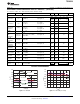
Table 3. PIN DESCRIPTION
PIN
NAME DESCRIPTION
NUMBER
1 NO Normally open
2 GND Digital ground
3 NC Normally closed
4 COM Common
5 V
+
Power supply
6 IN Digital control to connect COM to NO
Table 4. PARAMETER DESCRIPTION
SYMBOL DESCRIPTION
V
COM
Voltage at COM
V
NC
Voltage at NC
V
NO
Voltage at NO
r
on
Resistance between COM and NO ports when the channel is ON
r
peak
Peak on-state resistance over a specified voltage range
Δr
on
Difference of r
on
between channels in a specific device
r
on(flat)
Difference between the maximum and minimum value of r
on
in a channel over the specified range of conditions
Leakage current measured at the NC port, with the corresponding channel (NC to COM) in the OFF state under worst-
I
NC(OFF)
case input and output conditions
I
NC(PWROFF)
Leakage current measured at the NC port during the power-off condition, V
+
= 0
I
NO(OFF)
Leakage current measured at the NO port, with the corresponding channel (NO to COM) in the OFF state
I
NO(PWROFF)
Leakage current measured at the NO port during the power-off condition, V
+
= 0
Leakage current measured at the NC port, with the corresponding channel (NC to COM) in the ON state and the output
I
NC(ON)
(COM) open
Leakage current measured at the NO port, with the corresponding channel (NO to COM) in the ON state and the output
I
NO(ON)
(COM) open
Leakage current measured at the NO port, with the corresponding channel (NO to COM) in the OFF state and the output
I
NO(OFF)
(COM) open
Leakage current measured at the NO port, with the corresponding channel (NO to COM) in the ON state and the output
I
NO(ON)
(COM) open
I
COM(OFF)
Leakage current measured at the COM port, with the corresponding channel (COM to NO) in the OFF state
I
COM(PWROFF)
Leakage current measured at the COM port during the power-off condition, V
+
= 0
Leakage current measured at the COM port, with the corresponding channel (COM to NO) in the ON state and the output
I
COM(ON)
(NO) open
V
IH
Minimum input voltage for logic high for the control input (IN)
V
IL
Maximum input voltage for logic low for the control input (IN)
V
I
Voltage at the control input (IN)
I
IH
, I
IL
Leakage current measured at the control input (IN)
Turn-on time for the switch. This parameter is measured under the specified range of conditions and by the propagation
t
ON
delay between the digital control (IN) signal and analog output (COM or NO) signal when the switch is turning ON.
Turn-off time for the switch. This parameter is measured under the specified range of conditions and by the propagation
t
OFF
delay between the digital control (IN) signal and analog output (COM or NO) signal when the switch is turning OFF.
Make-before-break time. This parameter is measured under the specified range of conditions and by the propagation delay
t
MBB
between the output of two adjacent analog channels (NC and NO) when the control signal changes state.
Charge injection is a measurement of unwanted signal coupling from the control (IN) input to the analog (NO or COM)
Q
C
output. This is measured in coulomb (C) and measured by the total charge induced due to switching of the control
input.Charge injection, Q
C
= C
L
× ΔV
COM
, C
L
is the load capacitance and ΔV
COM
is the change in analog output voltage.
C
NC(OFF)
Capacitance at the NC port when the corresponding channel (NC to COM) is OFF
C
NO(OFF)
Capacitance at the NO port when the corresponding channel (NO to COM) is OFF
C
NC(ON)
Capacitance at the NC port when the corresponding channel (NC to COM) is ON
14 Submit Documentation Feedback Copyright © 2005–2012, Texas Instruments Incorporated
Product Folder Link(s): TS5A3160