
Datasheet


TS5A3154
SCDS191C –MARCH 2005– REVISED FEBRUARY 2012
www.ti.com
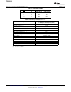
Electrical Characteristics for 5-V Supply
(1)
V
+
= 4.5 V to 5.5 V, T
A
= –40°C to 85°C (unless otherwise noted)
PARAMETER SYMBOL TEST CONDITIONS T
A
V
+
MIN TYP MAX UNIT
Analog Switch
Analog signal V
COM
, V
NO
,
0 V
+
V
range V
NC
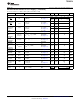
25°C 0.9 1.1
Peak ON 0 ≤ (V
NO
or V
NC
) ≤ V
+
, Switch ON,
r
peak
4.5 V Ω
resistance I
COM
= –100 mA, See Figure 13
Full 1.3
25°C 0.8 0.9
ON-state V
NO
or V
NC
= 2.5 V, Switch ON,
r
on
4.5 V Ω
resistance I
COM
= –100 mA, See Figure 13
Full 1.1
ON-state 25°C 0.05 0.1
resistance
V
NO
or V
NC
= 2.5 V, Switch ON,
matching Δr
on
4.5 V Ω
I
COM
= –100 mA, See Figure 13
Full 0.1
between
channels
25°C 0.15
0 ≤ (V
NO
or V
NC
) ≤ V
+
, Switch ON,
I
COM
= –100 mA, See Figure 13
ON-state Full
resistance r
on(flat)
4.5 V Ω
V
NO
or V
NC
= 1 V, 1.5 V, 25°C 0.09 0.15
Switch ON,
flatness
2.5 V,
See Figure 13
Full 0.15
I
COM
= –100 mA,
V
NC
or V
NO
= 1 V, 25°C –20 2 20
V
COM
= 4.5 V,
I
NC(OFF)
, Switch OFF,
or 5.5 V nA
NC, NO
I
NO(OFF)
See Figure 14
Full –150 150
V
NC
or V
NO
= 4.5 V,
OFF leakage
V
COM
= 1 V,
current
25°C –5 0.7 5
I
NC(PWROFF)
, V
NC
or V
NO
= 0 to 5.5 V, Switch OFF,
0 V μA
I
NO(PWROFF)
V
COM
= 5.5 V to 0, See Figure 14
Full –25 25
V
NC
or V
NO
= 1 V, 25°C –20 2 20
NC, NO V
COM
= Open,
I
NC(ON)
, Switch ON,
ON leakage or 5.5 V nA
I
NO(ON)
See Figure 15
Full –150 150
current V
NC
or V
NO
= 4.5 V,
V
COM
= Open,
V
COM
= 1 V, V
NC
or 25°C –20 2 20
V
NO
= 4.5 V,
Switch OFF,
I
COM(OFF)
or 5.5 V nA
COM
See Figure 14
Full –150 150
V
COM
= 4.5 V,
OFF leakage
V
NC
or V
NO
= 1 V,
current
25°C –5 0.7 5
V
NC
or V
NO
= 0 to 5.5 V, Switch OFF,
I
COM(PWROFF)
0 V μA
V
COM
= 5.5 V to 0, See Figure 14
Full –25 25
V
COM
= 1 V, 25°C –20 2 20
COM V
NC
or V
NO
= Open,
Switch ON,
ON leakage I
COM(ON)
or 5.5 V nA
See Figure 15
Full –150 150
current V
COM
= 4.5 V,
V
NC
or V
NO
= Open,
Digital Control Inputs (IN, EN)
(2)
Input logic high V
IH
Full 2.4 5.5 V
Input logic low V
IL
Full 0 0.8 V
25°C –100 25 100
Input leakage
I
IH
, I
IL
V
I
= 5.5 V or 0 V 5.5 V nA
current
Full –100 100
(1) The algebraic convention, whereby the most negative value is a minimum and the most positive value is a maximum.
(2) All unused digital inputs of the device must be held at V
+
or GND to ensure proper device operation. Refer to the TI application report,
Implications of Slow or Floating CMOS Inputs, literature number SCBA004.
4 Submit Documentation Feedback Copyright © 2005–2012, Texas Instruments Incorporated
Product Folder Link(s): TS5A3154