
Datasheet


TS5A3154
www.ti.com
SCDS191C –MARCH 2005– REVISED FEBRUARY 2012
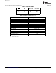
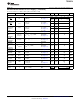
Absolute Minimum and Maximum Ratings
(1) (2)
over operating free-air temperature range (unless otherwise noted)
MIN MAX UNIT
V
+
Supply voltage range
(3)
–0.5 6.5 V
V
NC
,
V
NO
, Analog voltage range
(3) (4) (5)
–0.5 V
+
+ 0.5 V
V
COM
I
K
Analog port diode current V
NC
, V
NO
, V
COM
< 0 or V
NO
, V
NC
, V
COM
> V
+
–50 50 mA
I
NC
, On-state switch current –200 200
I
COM
, V
NC
, V
NO
, V
COM
= 0 to V
+
mA
On-state peak switch current
(6)
–400 400
I
NO
V
I
Digital input voltage range
(3) (4)
–0.5 6.5 V
I
IK
Digital input clamp current V
I
< 0 –50 mA
I
+
Continuous current through V
+
100 mA
I
GND
Continuous current through GND –100 100 mA
DCU package 227
θ
JA
Package thermal impedance
(7)
°C/W
YZP package 102
T
stg
Storage temperature range –65 150 °C
(1) Stresses above these ratings may cause permanent damage. Exposure to absolute maximum conditions for extended periods may
degrade device reliability. These are stress ratings only, and functional operation of the device at these or any other conditions beyond
those specified is not implied.
(2) The algebraic convention, whereby the most negative value is a minimum and the most positive value is a maximum
(3) All voltages are with respect to ground, unless otherwise specified.
(4) The input and output voltage ratings may be exceeded if the input and output clamp-current ratings are observed.
(5) This value is limited to 5.5 V maximum.
(6) Pulse at 1-ms duration < 10% duty cycle.
(7) The package thermal impedance is calculated in accordance with JESD 51-7.
Copyright © 2005–2012, Texas Instruments Incorporated Submit Documentation Feedback 3
Product Folder Link(s): TS5A3154