
Datasheet


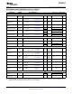


Table Of Contents
- FEATURES
- APPLICATIONS
- DESCRIPTION/ORDERING INFORMATION
- ABSOLUTE MAXIMUM RATINGS
- ELECTRICAL CHARACTERISTICS FOR 5-V SUPPLY
- ELECTRICAL CHARACTERISTICS FOR 3.3-V SUPPLY
- ELECTRICAL CHARACTERISTICS FOR 2.5-V SUPPLY
- ELECTRICAL CHARACTERISTICS FOR 1.8-V SUPPLY
- TYPICAL CHARACTERISTICS
- PARAMETER MEASUREMENT INFORMATION

ABSOLUTE MAXIMUM RATINGS
(1)
TS5A23157
SCDS165D – MAY 2004 – REVISED MAY 2008 ................................................................................................................................................................
www.ti.com
SUMMARY OF CHARACTERISTICS
2:1 Multiplexer/Demultiplexer
Configuration
(2 × SPDT)
Number of channels 2
ON-state resistance (r
on
) 10 Ω
ON-state resistance match
0.15 Ω
between channels ( Δ r
on
)
ON-state resistance flatness
4 Ω
(r
on(flat)
)
Turn-on/turn-off time (t
ON
/t
OFF
) 5.7 ns/3.8 ns
Break-before-make time (t
BBM
) 0.5 ns
Charge injection (Q
C
) 7 pC
Bandwidth (BW) 220 MHz
OFF isolation (OSIO) – 65 dB at 10 MHz
Crosstalk 9XTALK) – 66 dB at 10 MHz
Total harmo nic distortion (THD) 0.01%
Leakage current
± 1 µ A
(I
COM(OFF)
/I
NC(OFF)
)
Package options 10-pin DGS and RSE
over operating free-air temperature range (unless otherwise noted)
MIN MAX UNIT
V
+
Supply voltage range
(2)
– 0.5 6.5 V
V
NC
V
NO
Analog voltage range
(2) (3) (4)
– 0.5 V
+
+ 0.5 V
V
COM
V
NC
, V
NO
, V
COM
< 0 or V
NC
, V
NO
,
I
I/OK
Analog port diode current ± 50 mA
V
COM
> V
+
I
NC
I
NO
On-state switch current V
NC
, V
NO
, V
COM
= 0 to V
+
± 50 mA
I
COM
V
IN
Digital input voltage range
(2) (3)
– 0.5 6.5 V
I
IK
Digital input clamp current V
IN
< 0 – 50 mA
Continuous current through V
+
or GND ± 100 mA
DGS package 56.5
θ
JA
Package thermal impedance
(5)
° C/W
RSE package 243
T
stg
Storage temperature range – 65 150 ° C
(1) Stresses beyond those listed under "absolute maximum ratings" may cause permanent damage to the device. These are stress ratings
only, and functional operation of the device at these or any other conditions beyond those indicated under "recommended operating
conditions" is not implied. Exposure to absolute-maximum-rated conditions for extended periods may affect device reliability.
(2) All voltages are with respect to ground, unless otherwise specified.
(3) The input and output voltage ratings may be exceeded if the input and output clamp-current ratings are observed.
(4) This value is limited to 5.5 V maximum.
(5) The package thermal impedance is calculated in accordance with JESD 51-7.
2 Submit Documentation Feedback Copyright © 2004 – 2008, Texas Instruments Incorporated
Product Folder Link(s): TS5A23157