
Datasheet


A
EN (see Note A)
B
Charge
Pump
V
CC
D−
D+
1D−
1D+
2D−
2D+
S
OE
TS3USB221E
SCDS263B –SEPTEMBER 2009–REVISED JULY 2012
www.ti.com
ORDERING INFORMATION
T
A
PACKAGE
(1) (2)
ORDERABLE PART NUMBER TOP-SIDE MARKING
SON – DRC Reel of 3000 TS3USB221EDRCR ZVM
–40°C to 85°C
QFN (μQFN) – RSE Reel of 3000 TS3USB221ERSER LGR or LGO
(1) Package drawings, thermal data, and symbolization are available at www.ti.com/packaging.
(2) For the most current package and ordering information, see the Package Option Addendum at the end of this document, or see the TI
website at www.ti.com.
Table 1. PIN DESCRIPTION
NAME DESCRIPTION
OE Bus-switch enable
S Select input
D Bus A
nD Bus B
Table 2. TRUTH TABLE
S OE FUNCTION
X H Disconnect
L L D = 1D
H L D = 2D
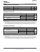
BLOCK DIAGRAM
Figure 1. SIMPLIFIED SCHEMATIC, EACH FET SWITCH (SW)
A. EN is the internal enable signal applied to the switch.
2 Submit Documentation Feedback Copyright © 2009–2012, Texas Instruments Incorporated
Product Folder Link(s): TS3USB221E