
Datasheet


TRS3243E
www.ti.com
SLLS789C –APRIL 2007– REVISED SEPTEMBER 2011
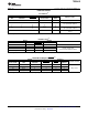
Absolute Maximum Ratings
(1)
over operating free-air temperature range (unless otherwise noted)
MIN MAX UNIT
V
CC
Supply voltage range
(2)
–0.3 6 V
V+ Positive output supply voltage range
(2)
–0.3 7 V
V– Negative output supply voltage range
(2)
0.3 –7 V
V+ – V– Output supply voltage difference
(2)
13 V
Driver (FORCEOFF, FORCEON) –0.3 6
V
I
Input voltage range V
Receiver –25 25
Driver –13.2 13.2
V
O
Output voltage range V
Receiver (INVALID) –0.3 V
CC
+ 0.3
DB package 62
θ
JA
Package thermal impedance
(3) (4)
DW package 46 °C/W
PW package 62
Lead temperature 1,6 mm (1/16 in) from case for 10 s 260 °C
T
stg
Storage temperature range –65 150 °C
(1) Stresses beyond those listed under "absolute maximum ratings" may cause permanent damage to the device. These are stress ratings
only, and functional operation of the device at these or any other conditions beyond those indicated under "recommended operating
conditions" is not implied. Exposure to absolute-maximum-rated conditions for extended periods may affect device reliability.
(2) All voltages are with respect to network GND.
(3) Maximum power dissipation is a function of T
J
(max), θ
JA
, and T
A
. The maximum allowable power dissipation at any allowable ambient
temperature is P
D
= (T
J
(max) - T
A
)/θ
JA
. Operating at the absolute maximum T
J
of 150°C can affect reliability.
(4) The package thermal impedance is calculated in accordance with JESD 51-7.
Recommended Operating Conditions
(1)
See Figure 6
MIN NOM MAX UNIT
V
CC
= 3.3 V 3 3.3 3.6
Supply voltage V
V
CC
= 5 V 4.5 5 5.5
V
CC
= 3.3 V 2
V
IH
Driver and control high-level input voltage DIN, FORCEOFF, FORCEON V
V
CC
= 5 V 2.4
V
IL
Driver and control low-level input voltage DIN, FORCEOFF, FORCEON 0.8 V
V
I
Driver and control input voltage DIN, FORCEOFF, FORCEON 0 5.5 V
V
I
Receiver input voltage –25 25 V
TRS3243EC 0 70
T
A
Operating free-air temperature °C
TRS3243EI –40 85
(1) Test conditions are C1–C4 = 0.1 μF at V
CC
= 3.3 V ± 0.3 V; C1 = 0.047 μF, C2–C4 = 0.33 μF at V
CC
= 5 V ± 0.5 V.
Electrical Characteristics
(1)
over recommended ranges of supply voltage and operating free-air temperature (unless otherwise noted) (see Figure 6)
PARAMETER TEST CONDITIONS MIN TYP
(2)
MAX UNIT
I
I
Input leakage current FORCEOFF, FORCEON ±0.01 ±1 μA
No load,
Auto-powerdown disabled 0.3 1 mA
FORCEOFF and FORCEON at V
CC
Powered off No load, FORCEOFF at GND 1 10
Supply current
I
CC
No load, FORCEOFF at V
CC
,
(T
A
= 25°C)
μA
FORCEON at GND,
Auto-powerdown enabled 1 10
All RIN are open or grounded,
All DIN are grounded
(1) Test conditions are C1–C4 = 0.1 μF at V
CC
= 3.3 V ± 0.3 V; C1 = 0.047 μF, C2–C4 = 0.33 μF at V
CC
= 5 V ± 0.5 V.
(2) All typical values are at V
CC
= 3.3 V or V
CC
= 5 V, and T
A
= 25°C.
Copyright © 2007–2011, Texas Instruments Incorporated Submit Documentation Feedback 5
Product Folder Link(s): TRS3243E