
Datasheet


SIP-8
(TOP VIEW)
SIP-8
(BOTTOMVIEW)
A1
B1
C1
A2
B2
C2
GND
MODE
VOUT
GND
A3
C3
VIN
EN
A3
C3
A2
B2
C2
GND
EN
VIN
GND
C1
VOUT
MODE
A1
B1
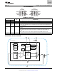
Gate Driver
Anti
Shoot-Through
Power Save Mode
Feedback Divider
+
-
Frequency
Control
R
1
R
2
L
GND
Soft-Start
EN VIN
Current Limit
Detect
Undervoltage
Lockout
Bias Supply
Bandgap
Thermal
Shutdown
Negative Inductor
Current Detect
VIN
MODE
V = 0.8 V
RE F
V
REF
C
I
1µH
C
4.7µF
O
Switching
VOUT
DC/DC CONVERTER
4.7µF
TPS82690
TPS82695
TPS82697
www.ti.com
SLVSA66B –JUNE 2011– REVISED FEBRUARY 2012
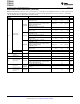
PIN ASSIGNMENTS
TERMINAL FUNCTIONS
TERMINAL
I/O DESCRIPTION
NAME NO.
VOUT A1 O Power output pin. Apply output load between this pin and GND.
VIN A2, A3 I The VIN pins supply current to the TPS8269xSIP's internal regulator.
This is the enable pin of the device. Connecting this pin to ground forces the converter into
EN B2 I shutdown mode. Pulling this pin to V
I
enables the device. This pin must not be left floating and
must be terminated.
This is the mode selection pin of the device. This pin must not be left floating and must be
terminated.
MODE = LOW: The device is operating in regulated frequency pulse width modulation mode
MODE B1 I
(PWM) at high-load currents and in pulse frequency modulation mode (PFM) at light load
currents.
MODE = HIGH: Low-noise mode enabled, regulated frequency PWM operation forced.
GND C1, C2, C3 – Ground pin.
FUNCTIONAL BLOCK DIAGRAM
Copyright © 2011–2012, Texas Instruments Incorporated Submit Documentation Feedback 5
Product Folder Link(s): TPS82690 TPS82695 TPS82697