
Datasheet


TPS82670, TPS82671, TPS82672, TPS82673, TPS82674
TPS82675, TPS82676, TPS82677, TPS826711, TPS826745, TPS826765
SLVSAI0F –OCTOBER 2010–REVISED NOVEMBER 2012
www.ti.com
APPLICATION INFORMATION
INPUT CAPACITOR SELECTION
Because of the pulsating input current nature of the buck converter, a low ESR input capacitor is required to
prevent large voltage transients that can cause misbehavior of the device or interference in other circuits in the
system.
For most applications, the input capacitor that is integrated into the TPS8267x should be sufficient. If the
application exhibits a noisy or erratic switching frequency, experiment with additional input ceramic capacitance
to find a remedy.
The TPS8267x uses a tiny ceramic input capacitor. When a ceramic capacitor is combined with trace or cable
inductance, such as from a wall adapter, a load step at the output can induce ringing at the VIN pin. This ringing
can couple to the output and be mistaken as loop instability or can even damage the part. In this circumstance,
additional "bulk" capacitance, such as electrolytic or tantalum, should be placed between the input of the
converter and the power source lead to reduce ringing that can occur between the inductance of the power
source leads and C
I
.
OUTPUT CAPACITOR SELECTION
The advanced, fast-response, voltage mode, control scheme of the TPS8267x allows the use of a tiny ceramic
output capacitor (C
O
). For most applications, the output capacitor integrated in the TPS8267x is sufficient.
At nominal load current, the device operates in PWM mode; the overall output voltage ripple is the sum of the
voltage step that is caused by the output capacitor ESL and the ripple current that flows through the output
capacitor impedance. At light loads, the output capacitor limits the output ripple voltage and provides holdup
during large load transitions.
The TPS8267x is designed as a Point-Of-Load (POL) regulator, to operate stand-alone without requiring any
additional capacitance. Adding a 2.2μF ceramic output capacitor (X7R or X5R dielectric) generally works from a
converter stability point of view, but does not necessarily help to minimize the output ripple voltage.
For best operation (i.e. optimum efficiency over the entire load current range, proper PFM/PWM auto transition),
the TPS8267xSIP requires a minimum output ripple voltage in PFM mode. The typical output voltage ripple is ca.
1% of the nominal output voltage V
O
. The PFM pulses are time controlled resulting in a PFM output voltage
ripple and PFM frequency that depends (first order) on the capacitance seen at the MicroSiP
TM
DC/DC
converter's output.
In applications requiring additional output bypass capacitors located close to the load, care should be taken to
ensure proper operation. If the converter exhibits marginal stability or erratic switching frequency, experiment
with additional low value series resistance (e.g. 50 to 100mΩ) in the output path to find a remedy.
Because the damping factor in the output path is directly related to several resistive parameters (e.g. inductor
DCR, power-stage r
DS(on)
, PWB DC resistance, load switches r
DS(on)
…) that are temperature dependant, the
converter small and large signal behavior must be checked over the input voltage range, load current range and
temperature range.
The easiest sanity test is to evaluate, directly at the converter’s output, the following aspects:
• PFM/PWM efficiency
• PFM/PWM and forced PWM load transient response
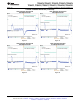
During the recovery time from a load transient, the output voltage can be monitored for settling time, overshoot or
ringing that helps judge the converter’s stability. Without any ringing, the loop has usually more than 45° of phase
margin.
20 Submit Documentation Feedback Copyright © 2010–2012, Texas Instruments Incorporated
Product Folder Links: TPS82670 TPS82671 TPS82672 TPS82673 TPS82674 TPS82675 TPS82676 TPS82677
TPS826711 TPS826745 TPS826765