
Datasheet


P
D
+
ǒ
V
IN
*V
OUT
Ǔ
@ I
OUT
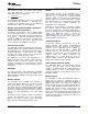
NOTES: A.Alllineardimensionsareinmillimeters.
B.Thisdrawingissubjecttochangewithoutnotice.
C.NanoStaräpackageconfiguration.
NanoStarisatrademarkofTexasInstruments.
1,427
1,327
1,060
0,960
(d=0.30 0.05)±
0,625Max
TPS799xx
SBVS056J –JANUARY 2005–REVISED AUGUST 2010
www.ti.com
THERMAL INFORMATION
The internal protection circuitry of the TPS799xx has
Thermal Protection
been designed to protect against overload conditions.
It was not intended to replace proper heatsinking.
Thermal protection disables the output when the
Continuously running the TPS799xx into thermal
junction temperature rises to approximately +165°C,
shutdown will degrade device reliability.
allowing the device to cool. When the junction
temperature cools to approximately +145°C the
output circuitry is again enabled. Depending on power Power Dissipation
dissipation, thermal resistance, and ambient
The ability to remove heat from the die is different for
temperature, the thermal protection circuit may cycle
each package type, presenting different
on and off. This cycling limits the dissipation of the
considerations in the PCB layout. The PCB area
regulator, protecting it from damage due to
around the device that is free of other components
overheating.
moves the head from the device to the ambient air.
Any tendency to activate the thermal protection circuit Performance data for JEDEC low- and high-K boards
indicates excessive power dissipation or an are given in the Dissipation Ratings table. Using
inadequate heatsink. For reliable operation, junction heavier copper will increase the effectiveness in
temperature should be limited to +125°C maximum. removing heat from the device. The addition of plated
To estimate the margin of safety in a complete design through-holes to heat-dissipating layers will also
(including heatsink), increase the ambient improve the heatsink effectiveness.
temperature until the thermal protection is triggered;
Power dissipation depends on input voltage and load
use worst-case loads and signal conditions. For good
conditions. Power dissipation is equal to the product
reliability, thermal protection should trigger at least
of the output current time the voltage drop across the
+35°C above the maximum expected ambient
output pass element, as shown in Equation 2:
condition of your particular application. This
configuration produces a worst-case junction
(2)
temperature of +125°C at the highest expected
ambient temperature and worst-case load.
Package Mounting
Solder pad footprint recommendations for the
TPS799xx are available from the Texas Instruments'
web site at www.ti.com.
Figure 30. YZU Wafer Chip-Scale Package Dimensions (in mm)
12 Submit Documentation Feedback Copyright © 2005–2010, Texas Instruments Incorporated