
Datasheet


SLVS325C − MARCH 2001 − REVISED MAY 2002
www.ti.com
5
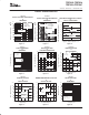
FUNCTIONAL BLOCK DIAGRAM—ADJUSTABLE VERSION
_
+
Thermal
Shutdown
Bandgap
Reference
V
IN
Current
Sense
R2
V
IN
GND
EN
V
OUT
SHUTDOWN
V
ref
UVLO
ILIM
External to
the Device
FB
R1
UVLO
250 kΩ
Bypass
FUNCTIONAL BLOCK DIAGRAM—FIXED VERSION
_
+
Thermal
Shutdown
V
IN
Current
Sense
R1
R2
V
IN
GND
EN
V
OUT
SHUTDOWN
V
ref
UVLO
ILIM
Bandgap
Reference
UVLO
250 kΩ
Bypass
Terminal Functions
TERMINAL
I/O
DESCRIPTION
NAME ADJ FIXED
I/O
DESCRIPTION
BYPASS 4 4 An external bypass capacitor, connected to this terminal, in conjunction with an internal resistor, creates
a low-pass filter to further reduce regulator noise.
EN 3 3 I The EN terminal is an input which enables or shuts down the device. When EN is a logic high, the device
will be in shutdown mode. When EN is a logic low, the device will be enabled.
FB 5 N/A I This terminal is the feedback input voltage for the adjustable device.
GND 2 2 Regulator ground
IN 1 1 I The IN terminal is the input to the device.
OUT 6 5 O The OUT terminal is the regulated output of the device.