
Datasheet


TPS77301/315/316/318/327/328/333/350 WITH RESET OUTPUT
TPS77401/415/418/427/428/433/450 WITH POWER GOOD OUTPUT
250-mA LDO REGULATORS WITH 8-PIN MSOP PACKAGING
SLVS281E – FEBRUARY 2000 – REVISED JULY 2001
2
POST OFFICE BOX 655303 • DALLAS, TEXAS 75265
description (continued)
Because the PMOS device behaves as a low-value resistor, the dropout voltage is very low (typically 200 mV
at an output current of 250 mA for 3.3-volt option) and is directly proportional to the output current. Additionally,
since the PMOS pass element is a voltage-driven device, the quiescent current is very low and independent
of output loading (typically 92 µA over the full range of output current, 0 mA to 250 mA). These two key
specifications yield a significant improvement in operating life for battery-powered systems.
The device is enabled when the EN
pin is connected to a low-level input voltage. This LDO family also features
a sleep mode; applying a TTL high signal to EN
(enable) shuts down the regulator, reducing the quiescent
current to less than 1 µA at T
J
= 25°C.
The TPS773xx features an integrated power-on reset, commonly used as a supply voltage supervisor (SVS),
or reset output voltage. The RESET
output of the TPS773xx initiates a reset in DSP, microcomputer or
microprocessor systems at power up and in the event of an undervoltage condition. An internal comparator in
the TPS773xx monitors the output voltage of the regulator to detect an undervoltage condition on the regulated
output voltage. When OUT
reaches 95% of its regulated voltage, RESET will go to a high-impedance state after
a 220-ms delay. RESET
will go to low-impedance state when OUT is pulled below 95% (i.e. over load condition)
of its regulated voltage.
For the TPS774xx, the power good terminal (PG) is an active high output, which can be used to implement a
power-on reset or a low-battery indicator. An internal comparator in the TPS774xx monitors the output voltage
of the regulator to detect an undervoltage condition on the regulated output voltage. When OUT
falls below 82%
of its regulated voltage, PG will go to a low-impedance state. PG will go to a high-impedance state when OUT
is above 82% of its regulated voltage.
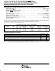
AVAILABLE OPTIONS
OUTPUT VOLTAGE (V) PACKAGED DEVICES MSOP (DGK)
T
J
TYP
TPS773xx
SYMBOL
TPS774xx
SYMBOL
5.0 TPS77350DGK AGN TPS77450DGK AGW
3.3 TPS77333DGK AGM TPS77433DGK AGV
2.8 TPS77328DGK AGK TPS77428DGK AGT
2.7 TPS77327DGK AGJ TPS77427DGK AGS
–40°C to 125°C
1.8 TPS77318DGK AGH TPS77418DGK AGQ
1.6 TPS77316DGK AWF — —
1.5 TPS77315DGK AGG TPS77415DGK AGP
Adjustable
1.5 V to 5.5 V
TPS77301DGK AGF TPS77401DGK AGO
NOTE: The TPS77301 and TPS77401 are programmable using an external resistor divider (see application information).
The DGK package is available taped and reeled. Add an R suffix to the device type (e.g., TPS77301DGKR).
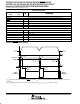
OUT
SENSE
6
5
3
IN
IN
EN
GND
4
7
1
V
I
0.1 µF
10 µF
+
OUT
8
V
O
PG or RESET Output
PG or
RESET
2
Figure 1. Typical Application Configuration (For Fixed Output Options)