
Datasheet


TPS735xx
SBVS087K –JUNE 2008–REVISED AUGUST 2013
www.ti.com
This integrated circuit can be damaged by ESD. Texas Instruments recommends that all integrated circuits be handled with
appropriate precautions. Failure to observe proper handling and installation procedures can cause damage.
ESD damage can range from subtle performance degradation to complete device failure. Precision integrated circuits may be more
susceptible to damage because very small parametric changes could cause the device not to meet its published specifications.
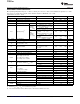
ORDERING INFORMATION
(1)
PRODUCT V
OUT
(2)
TPS735xx yyy z XX is nominal output voltage (for example, 28 = 2.8V, 285 = 2.85V, 01 = Adjustable).
YYY is package designator.
Z is package quantity.
(1) For the most current package and ordering information see the Package Option Addendum at the end of this document, or see the TI
website at www.ti.com.
(2) Output voltages from 1.0V to 3.6V in 50mV increments are available through the use of innovative factory EEPROM programming;
minimum order quantities may apply. Contact factory for details and availability.
ABSOLUTE MAXIMUM RATINGS
Over operating temperature range (unless otherwise noted).
(1)
PARAMETER TPS735xx UNIT
V
IN
range –0.3 to +7.0 V
V
EN
range –0.3 to V
IN
+0.3 V
V
OUT
range –0.3 to V
IN
+0.3 V
V
FB
range –0.3 to V
FB
(TYP) +0.3 V
Peak output current Internally limited
Continuous total power dissipation See Thermal Information table
Junction temperature range, T
J
–55 to +150 °C
Storage temperature range , T
STG
–55 to +150 °C
ESD rating, HBM 2 kV
ESD rating, CDM 500 V
(1) Stresses above these ratings may cause permanent damage. Exposure to absolute maximum conditions for extended periods may
degrade device reliability. These are stress ratings only, and functional operation of the device at these or any other conditions beyond
those specified is not implied.
2 Submit Documentation Feedback Copyright © 2008–2013, Texas Instruments Incorporated