
Datasheet


NOTES:A. V
RES
is the minimum input voltage for a valid RESET. The symbol V
RES
is not currently listed within EIA or JEDEC standards for
semiconductor symbology.
IN
V
RES
(see Note A)
V
RES
t
t
t
OUT
Threshold
Voltage
RESET
Output
50 ms
Delay
50 ms
Delay
Output
Undefined
Output
Undefined
V
IT+
(see Note B)
V
IT–
(see Note B)
V
IT+
(see Note B)
B. V
IT
–Trip voltage is typically 7% lower than the output voltage (93%V
O
) V
IT–
to V
IT+
is the hysteresis voltage.
V
IT–
(see Note B)
1.785
1.795
1.805
−40−25 −10 5 20 35 50 65 80 95 110 125
1.790
1.800
V
I
= 2.8 V
C
o
= 1 µF
T
J
− Junction Temperature − °C
− Output Voltage − V
V
O
I
O
= 1 A
I
O
= 0 mA
0 0.2 0.4 0.8
I
O
− Output Current − A
− Output Voltage − V
V
O
10.6
V
I
= 2.8 V
C
o
= 1 µF
T
J
= 25° C
1.7985
1.799
1.7995
1.8
1.8005
1.801
1.8015
0
50
100
150
200
250
−40 −25−10 5 20 35 50 65 80 95 110 125
T
J
− Junction Temperature − °C
Ground Current − Aµ
I
O
= 0 mA
V
I
= 2.8 V
C
o
= 1 µF
T
J
= 25° C
I
O
= 1 A
TPS72501
TPS72515, TPS72516
TPS72518, TPS72525
SLVS341E –MAY 2002–REVISED JUNE 2010
www.ti.com
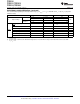
RESET TIMING DIAGRAM
TYPICAL CHARACTERISTICS
TPS72518 TPS72518 TPS72518
OUTPUT VOLTAGE OUTPUT VOLTAGE GROUND CURRENT
vs vs vs
OUTPUT CURRENT JUNCTION TEMPERATURE JUNCTION TEMPERATURE
Figure 1. Figure 2. Figure 3.
6 Submit Documentation Feedback Copyright © 2002–2010, Texas Instruments Incorporated
Product Folder Link(s): TPS72501 TPS72515 TPS72516 TPS72518 TPS72525