
Datasheet


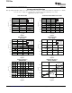


PIN CONFIGURATIONS
NOTE:(1)N/C=Notconnected.
IN
N/C
(1)
EN
6
5
4
OUT
NR/FB
GND
1
2
3
GND
TPS717xxDRV
2mmx2mmSON
(TOPVIEW)
TPS717xxDCK
SC70-5PACKAGE
(TOPVIEW)
OUT
NR/FB
IN
GND
EN
IN
N/C
(1)
EN
6
5
4
OUT
GND
NR/FB
1
2
3
TPS717xxDSE
1.5mmx1.5mmSON
(TOPVIEW)
1
2
3 4
5
TPS717xx
www.ti.com
.................................................................................................................................................. SBVS068G – FEBRUARY 2006 – REVISED APRIL 2009
Table 1. PIN DESCRIPTIONS
TPS717xx
1.5 × 1.5
SC70 2 × 2 SON SON
NAME (DCK) (DRV) (DSE) DESCRIPTION
IN 1 6 6 Input to the device.
GND 2 3 2 Ground.
Driving the enable pin (EN) high turns on the regulator. Driving this pin low puts the
EN 3 4 4
regulator into standby mode, thereby reducing operating current.
Fixed voltage versions only. An external capacitor connected to this terminal bypasses
NR 4 2 3
noise generated by the internal bandgap, lowering output noise.
Adjustable voltage version only. The voltage at this pin is fed to the error amplifier. A
FB 4 2 3
resistor divider from OUT to FB sets the output voltage when in regulation.
This is the regulated output voltage. A small capacitor is needed from this pin to ground
OUT 5 1 1
to assure stability; a 1.0 µ F ceramic capacitor is adequate.
NC – 5 5 Not connected. This pin can be tied to ground to improve thermal dissipation.
Copyright © 2006 – 2009, Texas Instruments Incorporated Submit Documentation Feedback 5