
Datasheet


1.8 V
2.8 V
5 V
OUTPUT VOLTAGE
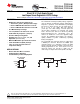
PROGRAMMING GUIDE
OUTPUT
VOLTAGE
R1 R2
3.16 MΩ
1 MΩ
1 MΩ
1 MΩ
V
O
V
I
FB
R1
R2
GND
IN
TPS71501
0.1 µF
0.47 µF
OUT
1.33 MΩ
0.499 MΩ
R1 +
ǒ
V
O
V
ref
* 1
Ǔ
R2
V
O
+ V
ref
ǒ
1 )
R1
R2
Ǔ
TPS71501-Q1
TPS71525-Q1, TPS71530-Q1
TPS71533-Q1, TPS71550-Q1
SGLS272G –OCTOBER 2004–REVISED JULY 2013
www.ti.com
Regulator Protection
The TPS715xx PMOS-pass transistor has a built-in back diode that conducts reverse current when the input
voltage drops below the output voltage (e.g., during power down). Current is conducted from the output to the
input and is not internally limited. If extended reverse voltage operation is anticipated, external limiting might be
appropriate.
The TPS715xx features internal current limiting. During normal operation, the TPS715xx limits output current to
approximately 500 mA. When current limiting engages, the output voltage scales back linearly until the
overcurrent condition ends. Take care not to exceed the power dissipation ratings of the package.
Programming the TPS71501 Adjustable LDO Regulator
The output voltage of the TPS71501 adjustable regulator is programmed using an external resistor divider as
shown in Figure 16. The output voltage is calculated using:
(3)
where:
V
REF
= 1.205 V typ (the internal reference voltage)
Resistors R1 and R2 should be chosen for approximately 1.5-μA divider current. Lower value resistors can be
used for improved noise performance, but the solution consumes more power. Higher resistor values should be
avoided as leakage current into/out of FB across R1/R2 creates an offset voltage that artificially
increases/decreases the feedback voltage and thus erroneously decreases/increases V
O
. The recommended
design procedure is to choose R2 = 1 MΩ to set the divider current at 1.5 μA and then calculate R1 using:
(4)
Figure 16. TPS71501 Adjustable LDO Regulator Programming
8 Submit Documentation Feedback Copyright © 2004–2013, Texas Instruments Incorporated
Product Folder Links: TPS71501-Q1 TPS71525-Q1 TPS71530-Q1 TPS71533-Q1 TPS71550-Q1