
Datasheet


www.ti.com
Detailed Description
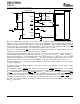
Pin Functions
Enable
Sequence
TPS70145, TPS70148
TPS70151, TPS70158
TPS70102
SLVS222D – DECEMBER 1999 – REVISED NOVEMBER 2004
DEVICE INFORMATION (continued)
Table 1. TERMINAL FUNCTIONS
TERMINAL
I/O DESCRIPTION
NAME NO.
EN 6 I Active low enable
GND 8 — Ground
MR1 4 I Manual reset input 1, active low, pulled up internally
MR2 5 I Manual reset input 2, active low, pulled up internally
NC 1, 11, 20 — No connection
Open drain output, low when V
OUT1
voltage is less than 95% of the nominal regulated
PG1 16 O
voltage
RESET 15 O Open drain output, SVS (power-on reset) signal, active low
Power-up sequence control: SEQ = High, V
OUT2
powers up first;
SEQ 7 I
SEQ = Low, V
OUT1
powers up first, SEQ terminal pulled up internally.
V
IN1
2, 3 I Input voltage of regulator 1
V
IN2
9, 10 I Input voltage of regulator 2
V
OUT1
18, 19 O Output voltage of regulator 1
V
OUT2
12, 13 O Output voltage of regulator 2
V
SENSE2
/FB2 14 I Regulator 2 output voltage sense/regulator 2 feedback for adjustable
V
SENSE1
/FB1 17 I Regulator 1 output voltage sense/regulator 1 feedback for adjustable
The TPS701xx low dropout regulator family provides dual regulated output voltages for DSP applications which
require high performance power management solutions. These devices provide fast transient response and high
accuracy with small output capacitors, while drawing low quiescent current. Programmable sequencing provides
a power solution for DSPs without any external component requirements. This reduces the component cost and
board space while increasing total system reliability. The TPS701xx family has an enable feature which puts the
device in sleep mode reducing the input currents to less than 3µA. Other features are integrated SVS (Power-On
Reset, RESET) and Power Good (PG1) that monitor output voltages and provide logic output to the system.
These differentiated features provide a complete DSP power solution.
The TPS701xx, unlike many other LDOs, feature very low quiescent current which remains virtually constant
even with varying loads. Conventional LDO regulators use a pnp pass element, the base current of which is
directly proportional to the load current through the regulator (I
B
= I
C
/ β ). The TPS701xx uses a PMOS transistor
to pass current; because the gate of the PMOS is voltage=driven, operating current is low and stable over the full
load range.
The EN terminal is an input which enables or shuts down the device. If EN is at a voltage high signal, the device
is in shutdown mode. When EN goes to voltage low, the device is enabled.
The SEQ terminal is an input that programs which output voltage (V
OUT1
or V
OUT2
) is turned on first. When the
device is enabled and the SEQ terminal is pulled high or left open, V
OUT2
turns on first and V
OUT1
remains off until
V
OUT2
reaches approximately 83% of its regulated output voltage. At that time, V
OUT1
is turned on. If V
OUT2
is
pulled below 83% (for example, an overload condition) V
OUT1
is turned off. These terminals have a 6µA pullup
current to V
IN1
.
Pulling the SEQ terminal low reverses the power-up order and V
OUT1
is turned on first. For detailed timing
diagrams, refer to Figure 40 through Figure 44 .
9