
Datasheet


www.ti.com
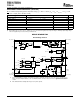
NOTES: A. V
RES
is the minimum input voltage for a valid RESET. The symbol V
RES
is not currently listed within EIA or JEDEC standards
for semiconductor symbology.
V
IN2
V
RES
(see Note A)
V
RES
t
t
t
V
OUT2
Threshold
Voltage
RESET
Output
120 ms
Delay
120 ms
Delay
Output
Undefined
Output
Undefined
V
IT+
(see Note B)
V
IT −
(see Note B)
V
IT+
(see Note B)
B. V
IT
−Trip voltage is typically 5% lower than the output voltage (95%V
O
) V
IT−
to V
IT+
is the hysteresis voltage.
V
IT −
(see Note B)
NOTES: A. V
PG1
is the minimum input voltage for a valid PG1. The symbol V
PG1
is not currently listed within EIA or JEDEC
standards for semiconductor symbology.
V
PG1
t
t
t
Threshold
Voltage
PG1
Output
Output
Undefined
Output
Undefined
V
IT+
(see Note B)V
IT+
(see Note B)
B. V
IT
−Trip voltage is typically 5% lower than the output voltage (95%V
O
) V
IT−
to V
IT+
is the hysteresis voltage.
V
IN1
V
OUT2
V
PG1
(see Note A)
V
IT −
(see Note B)
V
IT −
(see Note B)
V
UVLO
V
UVLO
TPS70145, TPS70148
TPS70151, TPS70158
TPS70102
SLVS222D – DECEMBER 1999 – REVISED NOVEMBER 2004
DEVICE INFORMATION (continued)
RESET Timing Diagram (with V
IN1
Powered Up)
PG1 Timing Diagram
8