
Datasheet


www.ti.com
V
OUT2
V
IN1
V
IN2
EN
SEQ
V
OUT1
V
SENSE1
PG1
MR2
RESET
MR1
V
SENSE2
V
OUT2
V
I
V
OUT1
MR1
0.1 µF
RESET
10 µF
10 µF
0.1 µF
MR2
EN
2 V
0.7 V
TPS701xxPWP
(Fixed Output Option)
>2 V
<0.7 V
250 kΩ
83%
95%
120ms
EN
V
OUT2
V
OUT1
PG1
MR1
MR2
(MR2 tied to PG1)
RESET
SEQ
120ms
83%
95%
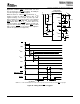
NOTE A: t1 − Time at which both V
OUT1
and V
OUT2
are greater than the PG1 thresholds and MR1 is logic high.
t1
(see Note A)
TPS70145, TPS70148
TPS70151, TPS70158
TPS70102
SLVS222D – DECEMBER 1999 – REVISED NOVEMBER 2004
Application condition: MR2 is tied to PG1, V
IN1
and
V
IN2
are tied to the same input voltage, the SEQ pin
is tied to logic high and MR1 is toggled.
When the device is enabled ( EN is pulled low), V
OUT2
begins to power up. When it reaches 83% of its
regulated voltage, V
OUT1
begins to power up. PG1
turns on when V
OUT1
reaches to 95% of its regulated
voltage, and since MR2 and PG1 are tied together,
MR2 follows PG1. When V
OUT1
reaches 95% of its
regulated voltage, the RESET switches to high volt-
age level after a 120ms delay. When MR1 is pulled
low, it causes RESET to go low, but the regulators
remains in regulation (see Figure 42 ).
Figure 42. Timing when MR1 is Toggled
23