
Datasheet


TPS65910
,
TPS65910A
,
TPS65910A3
,
TPS659101
TPS659102
,
TPS659103
,
TPS659104
,
TPS659105
TPS659106, TPS659107, TPS659108, TPS659109
SWCS046U –MARCH 2010–REVISED JUNE 2014
www.ti.com
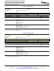
Table 6-49. BBCH_REG
Address Offset 0x39
Physical Address Instance
Description Back-up battery charger control register
Type RW
7 6 5 4 3 2 1 0
Reserved BBSEL BBCHEN
Bits Field Name Description Type Reset
7:4 Reserved Reserved bit RO 0x00
R returns
0s
2:1 BBSEL Back up battery charge voltage selection: RW 0x0
BBSEL[1:0] = 00 : 3.0 V
BBSEL[1:0] = 01 : 2.52 V
BBSEL[1:0] = 10 : 3.15 V
BBSEL[1:0] = 11 : VBAT
0 BBCHEN Back up battery charge enable RW 0
Table 6-50. DCDCCTRL_REG
Address Offset 0x3E
Physical Address Instance
Description DCDC control register
Type RW
7 6 5 4 3 2 1 0
Reserved VDD2_PSKIP VDD1_PSKIP VIO_PSKIP DCDCCKEXT DCDCCKSYNC
Bits Field Name Description Type Reset
7:6 Reserved Reserved bit RO 0x0
R returns
0s
5 VDD2_PSKIP VDD2 pulse skip mode enable (EEPROM bit) RW 1
4 VDD1_PSKIP VDD1 pulse skip mode enable (EEPROM bit) RW 1
3 VIO_PSKIP VIO pulse skip mode enable (EEPROM bit) RW 1
2 DCDCCKEXT This signal control the muxing of the GPIO0 pad: RW 0
When 0: this pad is a GPIO
When 1: this pad is used as input for an external clock used for the
synchronisation of the DCDCs
1:0 DCDCCKSYNC DCDC clock configuration: RW 0x3
DCDCCKSYNC[1:0] = 00 : no synchronization of DCDC clocks
DCDCCKSYNC[1:0] = 01 : DCDC synchronous clock with phase shift
DCDCCKSYNC[1:0] = 10 : no synchronization of DCDC clocks
DCDCCKSYNC[1:0] = 11 : DCDC synchronous clock
80 Detailed Description Copyright © 2010–2014, Texas Instruments Incorporated
Submit Documentation Feedback
Product Folder Links: TPS65910 TPS65910A TPS65910A3 TPS659101 TPS659102 TPS659103 TPS659104
TPS659105 TPS659106 TPS659107 TPS659108 TPS659109